This thread has been locked.

If you have a related question, please click the "Ask a related question" button in the top right corner. The newly created question will be automatically linked to this question.

TPS43351EVM: Sub-harmonic oscillation at high low and high VIN for 3.3V, 5A output

Part Number: TPS43351EVM
Other Parts Discussed in Thread: TPS43351-Q1

Hi Again,

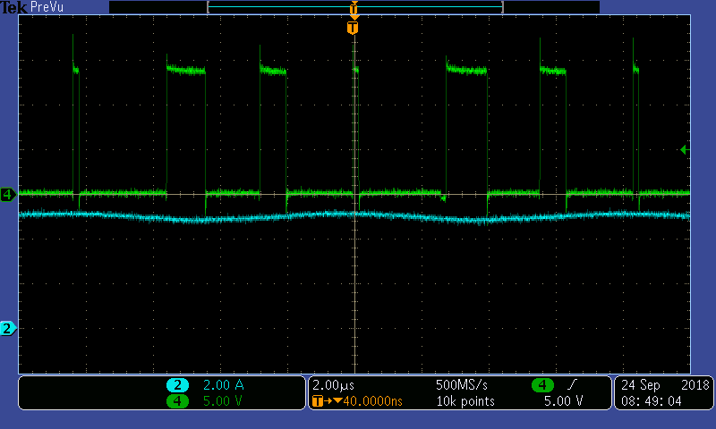
      I'm asking this question now because I wanted to be sure that frequency synchronization issues were not at fault. Now that those are resolved, I have the same circuit, now the output #4, Gordion has the complete schematics. For VIN above 12.0V and Iout above 3.5A, I see a progressively worse sub-harmonic osculation in the switch node duty cycle. Increasing VIN and/or Iout make this oscillation more and more pronounced.

Ch.2 = Iout, Ch.4 = SW node, this is for VIN = 13.8V and Iout = 5A (max load)

My first post about this IC led to two changes with the first TPS43351-Q1 on the board, those were to remove the resistor that connected the other output which is 5.0V to the EXTSUP pin and to increase the VREG pin capacitance to 4.7 uF. I have made those two changes to the second TPS43351 that generates this 3.3V, 5A output, but neither has stopped the oscillation.

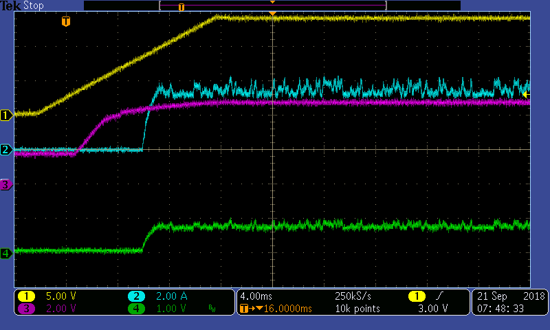
     In addition, I found that if I tried to start up into a load higher than 3.5A (constant current load), either by applying input power or by using the logic enable, the output would get stuck with a voltage of around 0.8V and delivering those 3.5A of average current. Here''s a plot of such a startup:

Ch.1 = VIN, Ch.2 = Iout, Ch.3 = ENA and ENB pins, Ch.4 = Vout

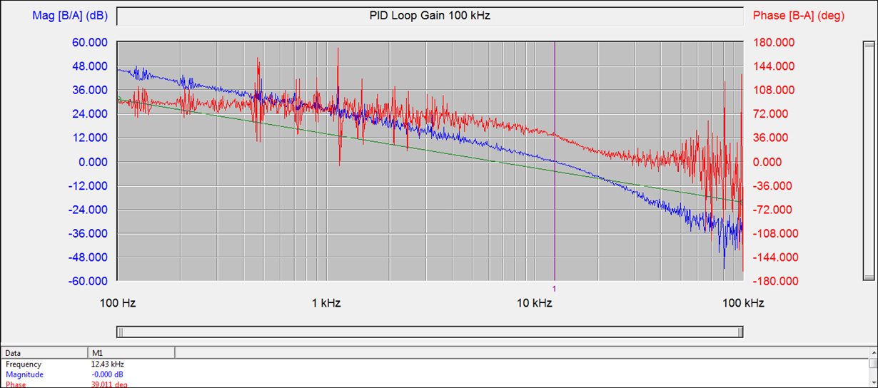
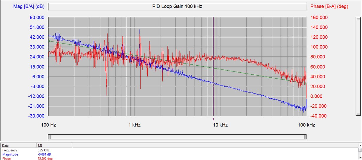
The solution to this was to lower the current sense resistance. In order to get a fairly smooth, monotonic startup, I had to reduce the current sense resistance to 2.5 mohm from its original 5 mohm. This caused some changes to the gain-phase response, so I also adjusted the control loop compensation. This is conservative but very stable:

Before there was some confusion about the phase margin - this is read directly, and is reported at the bottom: 75º at 8.3 kHz BW. This is with VIN = 13.8V and Iout = 3.0A. Above 3.5A the Bode plots are just noise.

     I have ruled out power supply impedance interaction at the input, mainly because this instability actually gets better as VIN drops - the opposite of what you would see if the input impedance was causing problems. And I've ruled out low phase margin or gain margin in the control loop. I don't really want to lower the current sense resistance further because I'm worried about signal-to-noise ratio. What else could cause the sub-harmonic oscillation?

     Thanks,

Chris

  • Chris,
    Are you using GB2 to drive SYNC of the second IC in this application? If yes, try removing GB2 and either use RT or drive the SYNC pin with an external circuit on the second IC.

    FYI: I's not a good idea to use GB2 to drive SYNC of the second IC.

    Are both IC's showing this sub-harmonic oscillation? or; just first IC? second IC?

    Is the spread spectrum in operation?
  • Hi Gordon,

         Yes, I'm using GB2, since I wanted the rising edge of the second TPS43351's Channel A to coincide with the rising edge of the first TPS43351's Channel B rising edge. I didn't realize that the RT pin signal could be used to sync the second IC. The GB2 signal is quite clean, you can see it here:

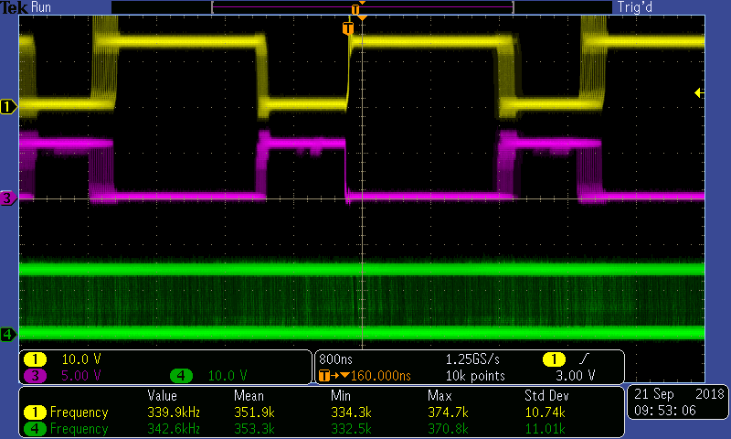
    Ch.1 = First IC's Channel B switch node, Ch.3 = GB2 of first IC (used as SYNC), Ch.4 = second IC's Channel A switch node

    I appreciate your concern about the possible radiated EMI impact of the GB2 trace, but the two IC's are close together and oriented such that this trace is short:

    It's the one called "SYNC", and the two vias on the left are just north of the GB2 pin, then the via on the far right is right next to the SYNC pin of the second IC. The trace is surrounded by PGND and also has a solid PGND plane underneath on both internal layers.

          This sub-harmonic oscillation only shows up in the 3.3V, 5A output. The other three outputs are clean (steady duty cycle) up to their maximum loads, over the full VIN range (quite narrow, just 10V to 16V). I am using spread spectrum, and in fact that's why it seemed like the synchronization wasn't working. However, as a test, I disabled the spread spectrum by removing a jumper that shorted the SYNC pin of the first IC to VREG, and then tested with and without the jumper that connected GB2 of the first IC to SYNC of the second:

    - With GB2 to SYNC jumper: both ICs in DCM at light load, then in CCM at heavy load, with proper sync between them. However the 3.3V, 5A output still showed sub-harmonic oscillation for Io > 3.5A and VIN > 12V

    - Without GB2 to SYNC jumper: both ICs in DCM at light load, then CCM at heavy load. Not synchronized. The 3.3V, 5A output still showed sub-harmonic oscillation for Io > 3.5A and VIN > 12V.

    I have concluded that the frequency sync is indeed working, and also that it's not responsible for the sub-harmonic oscillation in the 3.3V, 5A output.

    Since the voltage loop is nice and stable, I'm wondering if the peak current loop is unstable. I did have to reduce the current sense resistance to 2.5 mohm to ensure startup into a full load,, whereas the datasheet calculations say that 4.7 mohm would be perfect for optimum slope compensation.

    Thanks,

    Chris

  • Chris,

    No, the RT pin can't drive SYNC. I guess my statement was not very clear.

    (Try removing GB2 from the SYNC pin and either use the RT pin for the clock, or drive the SYNC pin with an external circuit on the second IC.)

    It looks like you are past this point, but I just wanted to clarify.

    I ran the math on the 4th rail (3.3V) and again, to me the COMP circuit looks wrong. I am pretty sure you have run a BODE plot on this. I guess the most important item I can think of is that the divider pole and second pole is quite low. It's possible that this could cause a low frequency ripple and potentially cause a full load startup issue.

    I have not seen this kind of ripple in the output except when the output circuit has a lot of capacitance with high ESR, and you don't have either.   

    I have tried to attach the math work sheet for the TPS433x. This is where I do my calculations when designing a board and supporting a customer, So far I have never had a problem when using these values. We do have other customers that use there own calculations and their COMP circuits are very different from ours, and they seem to work fine.

    slvc528.zip

    I sometimes put a 47pf across the top FB resistor. (in your case R41) This provides some feed forward compensation for fast load steps. Probably not your issue, but wanted to through it out there.

    Over all your design looks solid, the only difference between what you have and what I normally run is the COMP values. Take a look at the attached spread sheet and let me know what you think.

    In the mean time I will take an EVM and change the COMP components to match your values and see if I can get it to ripple like that.

  • Hi Gordon,

        Thanks for the clarification - I didn't think the RT pin could drive the SYNC pin of a second TPS43351. I have let each IC run free, and both do so happily, but no combination of free running or synchronizing them makes this sub-harmonic oscillation in Vo4 go away.

        While we're on this topic, how would you recommend synchronizing two TPS43351's together, given that both need spread spectrum?

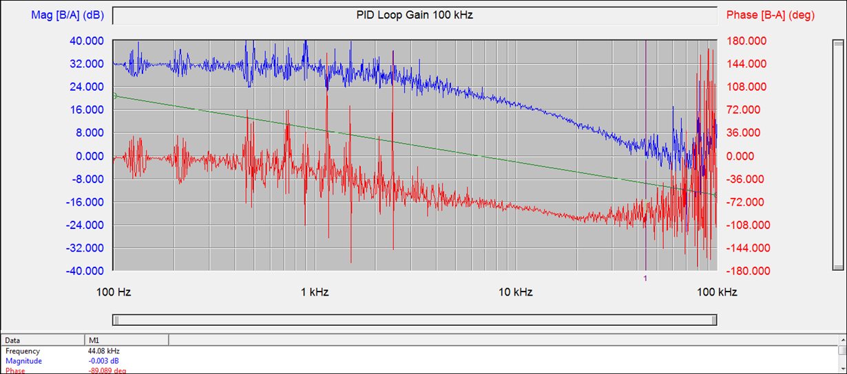
    I should have been clearer about my control loop compensation. Here's the result when the COMP values shown in the schematics I used were on the PCB:

    This is with VIN = 13.8V and Io = 3.0A. BW of 12 kHz, PM of 39º. That's a bit low for phase margin for my taste, so I took a plot of the power stage only, same conditions:

    Then I adjusted my guessed small signal model for current sense gain and slope comp amplitude until it was pretty close to this actual plot above. Then I recalculated the compensation and and targeted 10 kHz of BW. That led me to R36 = 649 ohms, C59 = 100 nF and C60 = 3.3 nF. The result was this, again for 13.8V input and 3.0A out:

    Slower, but very, very stable. Is it possible that low SNR on the current sense signal is responsible?

    Thanks,

    Chris

  • Chris,
    The recommended method of synchronizing two IC's is to use a separate clock source and drive both SYNC pins. This will allow the IC's to sync and spread spectrum to do it's own thing for each rail, providing the minimum radiated noise across 4 rails. Adding a separate circuit for this is not always possible. Some customers use a GPIO pin from a controller and setup an internal timer to set the frequency. This also allow them to steer the clock away from AM band interference once you have swept the radiated emissions and you know where the interference point is on the AM dial.
    Since the current measurement signal is approximately 50mV across the shunt, the SNR is definitely a possibility. That is why we recommend a capacitor across the shunt pins of the IC. We have even recommended two 10 Ohm resistors connected in series with the shunt lines. This with the capacitor on the shunt pins, creates a PIE filter for the shunt.

    Do you want to close this E2E question for now or keep it open for follow up on this question?
  • Hi Gordon,

          I had a feeling that the separate clock source was going to be the suggested manner, and it would be nice to offset each of the four outputs by 90º, but I don't think my customer would accept a hardware change purely for this reason.

          I can't say that the basic question is resolved yet because even when I let the oscillator of the IC that controls my 3.3V, 5A output run freely, I still see the sub-harmonic oscillation for input voltages above 12.0V and output currents above 3.5A. I have concluded that clock sync is not at fault.

          I'm not sure that SNR of the current sense signal is to blame, either, because I have a 5V, 6A output, called Vo2, and in order to get that output to start up into full load either by applying VIN or be a logic enable, I also had to reduce the current sense resistance to 2.5 mohm. That output shows no sub-harmonic oscillation of its duty cycle to the full 6A, over the full VIN range of 10V to 16V. The inductor values are different, but the different output voltages mean that for Vo2 the peak-to-peak sensed voltage is actually lower than the peak-to-peak sensed voltage of problematic Vo4. In theory SNR for Vo4 is higher.

         I'll take some scope shots of the voltages across the sense resistors of Vo2 and Vo4 for comparison and post them soon.

    Thanks,

    Chris

  • Hi Gordon,

         To begin, my apologies for taking so long to respond. I moved to a real office (a big step for me!) but that stopped all engineering cold for two weeks in a row.

    The sub-harmonic oscillation I saw was due to poor layout, purely my fault. The current sense resistor traces run right past the switch node with no electrostatic shield between the two, and that induces a significant vertical offset into the signal. It happens regardless of load, so I'm sure it's electric field coupling. If my customer lets me, I'll fix that in a new layout.

        Many thanks again for all your help!

    Chris