A related question is a question created from another question. When the related question is created, it will be automatically linked to the original question.
If you have a related question, please click the "Ask a related question" button in the top right corner. The newly created question will be automatically linked to this question.
Assuming there aren't any assembly issues it's hard to say without a schematic. Would you be willing to send one along for review? What voltages are sitting at 4V - PWM or the outputs?
Also, please check to ensure the IC and FETs are both soldered down correctly without shorts or bridges.
Hi! Thank you for your answer! The reason has been found. The "IN-" of the UCC27512(which is used to drive GAN FET on secondary) pull PWM1 and PWM2 to 4V. Adding a resistor of 24K from PWMX to GND resolving it.
But I have another question,I want to see the output waveform(PWM1,PWM2) of the chip, How to configure it? Now,the V5A,VDD and VINTF are OK,EN is high level, but PWM1 and PWM2 are low level. The input voltage of the converter is added to 6V,PWM2 has several pulse width and then disappears.How did the chip start?
Can you share a schematic with me please? It's hard to say what the fault was caused by without checking one over. There could be other connection issues like you've already found. Also, any scope shots of the failure would be useful too.
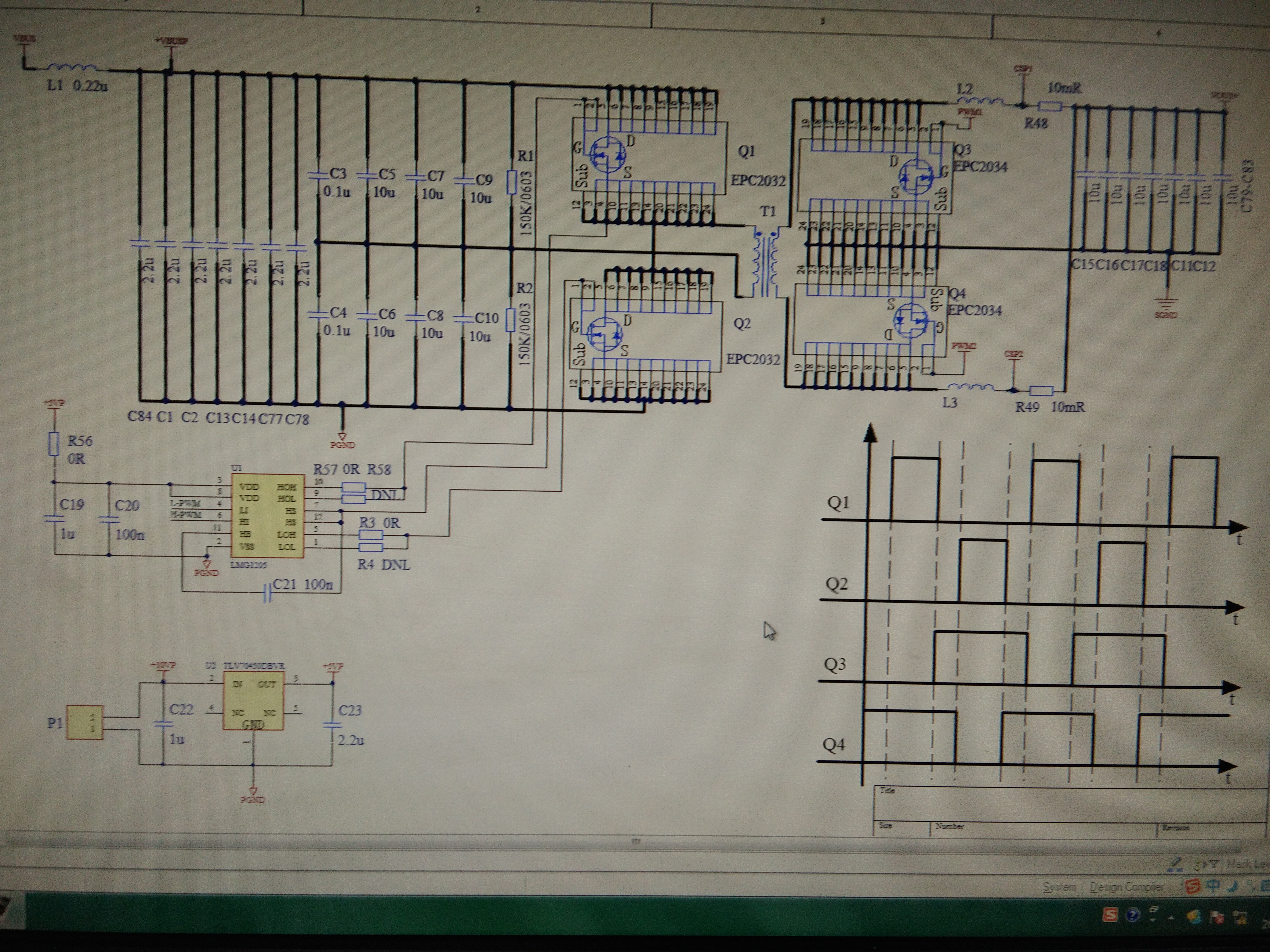
Hello! The first is the control part, and the second is the power part. VO is28V, IO is 10A, frequency is 1M. The primary driver chip is LMG1205. Current sampling uses INA139. What is the starting time sequence of TPS53632G? In other words, how to make the chip output with auxiliary power supply only?
Can you please share more information about what's going wrong and what you're trying to accomplish? Unfortunately it's not quite clear from you're posts. Certain voltages like VINTF, VO, and V5A aren't on your schematic. Also, what is the auxiliary supply you're trying to operate the controller on?
If you can share any scope captures of the failure with me along with more information on what you're trying to accomplish it would be a big help.
Hi!
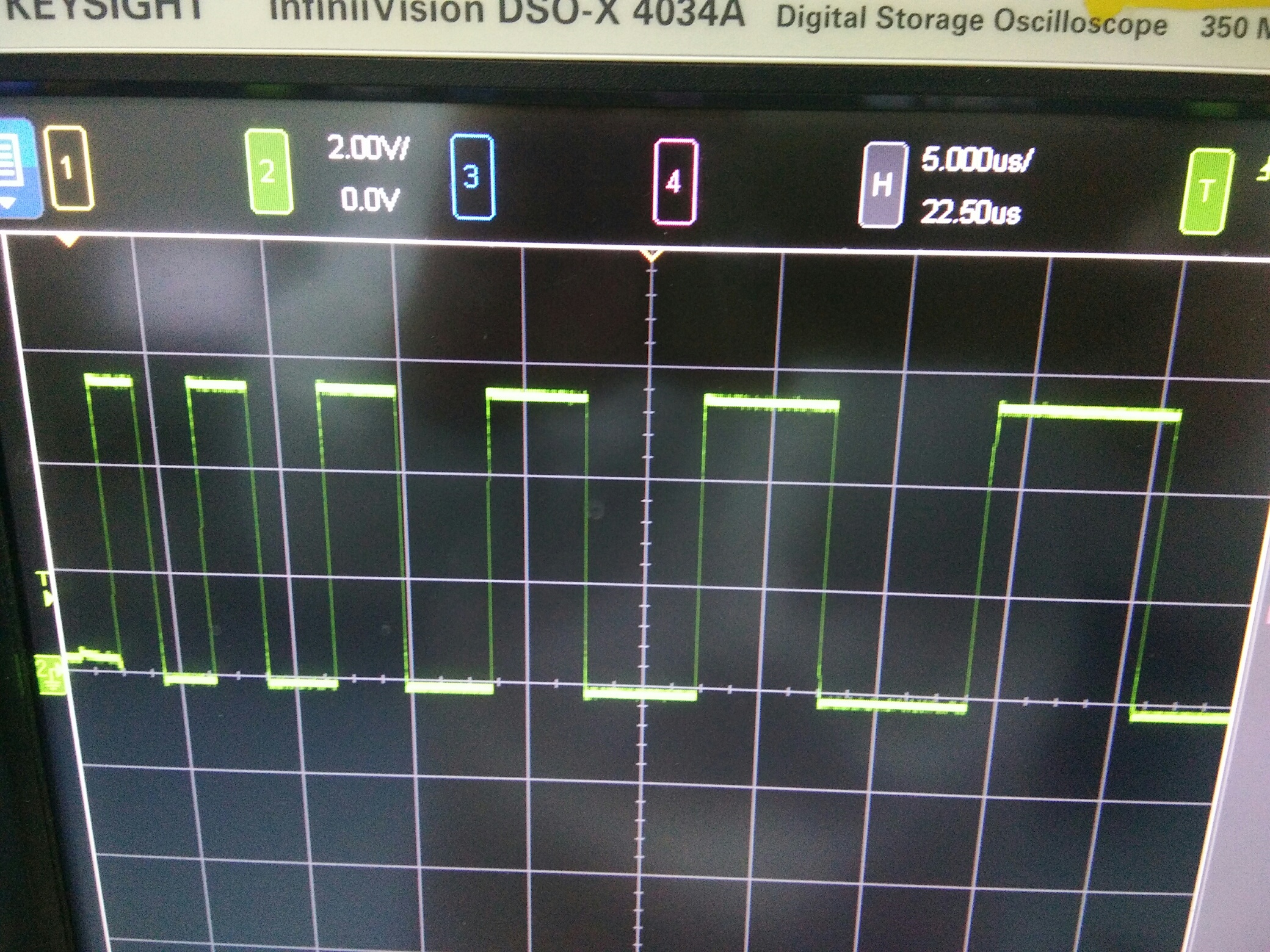
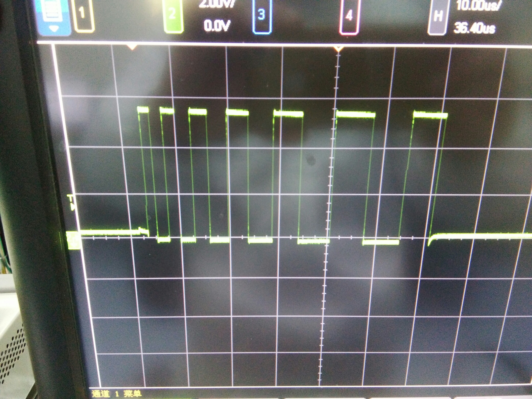
VO is the output voltage of the Converter ,It is designed 28V. V5A ,VDD and VINTF is the power supply of chip, they are corresponding to the 28, 2 and 14 pins of the chip respectively. What I am testing now is that the input of the converter is not added, After the auxiliary power is turned on, the voltage of the three legs is normal : V5A is 5V, VDD and VINTF is 3.3V, and the EN legs are high. At this time, PWM 1 and PWM 2 have several pulse width outputs, and then they are always low. Is it normal? Now I want to see the driving relationship between the four power transistors. I'll share with you some photos of the test later. What is the normal working condition of this chip?
The auxiliary power comes from a regulated power supply with a voltage value of 10V, which is converted to 5V and 3.3V through LDO. 5V power is supplied to V5A (pin 28)and 3.3V is supplied to VDD (pin2) and VINTF(pin 14). When these voltages are normal, the EN pin (pin 8) is pulled to a high level, and then PWM1 and PWM2 will have 7 pulse width outputs. The first is the partial output of the pin 6, the second is the total output of the pin 6, the third is the partial output of the pin 5, and the fourth is the total output of the pin 5. After 7 pulse width output, the two pins are always low.
The difference is that my design output is 28V, 10A. Current sensing is used resistance, the sample value is processed by INA139 and sent to the CSNx (pin18 and 19) and CSPx(pin17 and 20).
Thanks for sending along the scope caps and details. Just to make sure i'm reading your posts properly, can you please confirm the following:
Vout = 28V at 10A
Vin = ?
You would like to operate the converter without VIN present to verify functionality first
A 10V aux supply might be applied to VIN instead
Depending on which of those is true you may be violating the datasheet for the controller. On page 7 - EN can only be pulled high after 5V, 3.3V, and VIN are present. Otherwise the controller will likely detect a fault and shutdown after a few pulses which is what you're seeing.
Also, if your transformer turns step the voltage down from VIN then going from 10Vin to 28Vout is not possible.
The link to the TI Design you posted is broken unfortunately, can you please give me the number so I can look it up?
When Vin is 6V or not applied, the converter is not able to regulate Vout at 28V.
As a result, output undervoltage protection (UVP) happens and turn off PWM signal.
EN pin power recycle is needed to turn on PWM. Please refer to datasheet page 11 for UVP information.
I believe the purpose of your test is to check the deadtime betwen primary drive signal and secondary drive signal to prevent FET damage, but the test method without VIN applied does not work.
Here are some ideas to make Vout regulator to check dead time.
1. set Vout to a much lower voltage like 5V or lower, then you can apply lower Vin to make the converter work.
2. Apply a current limit on your Vin power supply to prevent FET damage.
3. Disconnect secondary drive signal, the secondary FET works as a diode. Converter is still able to regulate the Vout. When the controller is switching, you can check the primary and secondardy gate drive signal.
Hi! Thank you !
First, let me confirm your question:
1. As you said, Vout =28V at 10A.
2. Vin=36-75V.
3. Yes,I would like to operate the converter without VIN present to verify functionality first, and to check the deadtime betwen primary drive
signal and secondary drive signal to prevent FET damage.
4. Yes, 10V aux supply is applied to VIN instead. The purpose is to get the chip powered up.
Now, The EN pin is pulled up through the resistance of 10K to 3.3 V. This time, I 'll turn EN high after 3.3 V, 5V, and VIN are normal, and I 'll get back to you.
Just like you said, the purpose of my test is to check the deadtime betwen primary drive signal and secondary drive signal to prevent FET damage.I will do the test according to the method you provided, and then report the results back to you.
The test was conducted according to the method you provided: VIN is 7V, a current limit on Vin power supply is 0.3A, remove the secondary driver. when the output is set to 1V, there is 50 us pulse width, frequency is around 2M, the output voltage rises to 0.65 V, and then it is turned off. When the output is set to 3V, it works. But after the power was added, the FET at the bridge arm was broken. What could be the reason?
The test was conducted : VIN is 7V, a current limit on Vin power supply is 0.3A, remove the secondary driver. when the output is set to 1V, there is 50 us pulse width, frequency is around 2M, the output voltage rises to 0.65 V, and then it is turned off. When the output is set to 3V, it works. But after the power was added, the FET at the low bridge arm was broken. What could be the reason?
One more comment, when secondary drive signal is disconnected from FET, the secondary FET works as a diode, there is no dead time concern between primary and secondary.
you may need to apply some load to let PWM switch continuously, so you can check primary and secondary gate drive signal.
I'm sorry, but I didn't carry out the test because I was on a business trip last week. Your email address has been received. Today I will continue to carry out the test, and the test results will communicate with you.