Because of the Thanksgiving holiday in the U.S., TI E2E™ design support forum responses may be delayed from November 25 through December 2. Thank you for your patience.

This thread has been locked.

If you have a related question, please click the "Ask a related question" button in the top right corner. The newly created question will be automatically linked to this question.

UCC27538: OUTH protection

Part Number: UCC27538
Other Parts Discussed in Thread: UCC27531

Hi Ti

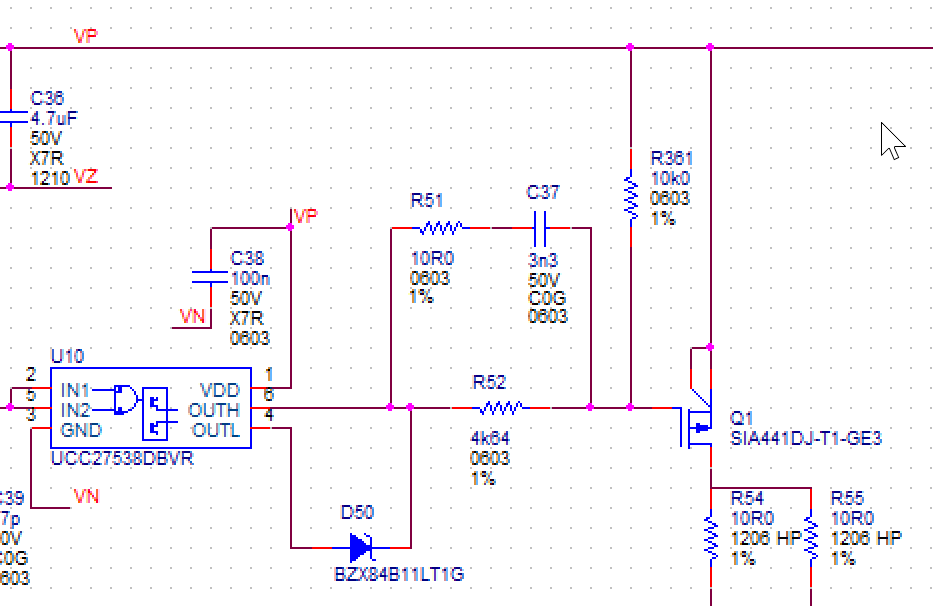
Is there some internal zener diode connected from OUTH to OUTL in UCC27538? (Similar to D50 in the schematic below)

It seems to pull OUTH down to ~8V, when input goes low, even though OUTL is left unconnected. (In below schematic it happens even though D50 is disconnected)

Can I damage the device by using this zener? (I switch with very low frequency <200Hz, and only charge a few nF through 10ohm)

See schematic below: (VP=21V, VN=0V)

Regards,

Tune

  • Hi Tune,

    Thanks for reaching to the High Power Drivers team, my name is Mamadou Diallo and I will help address your questions.

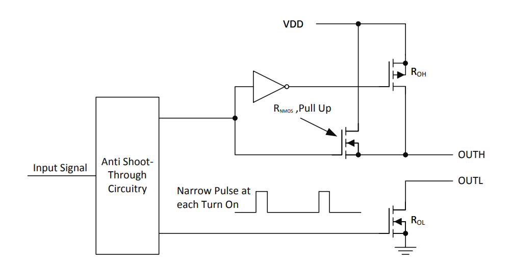
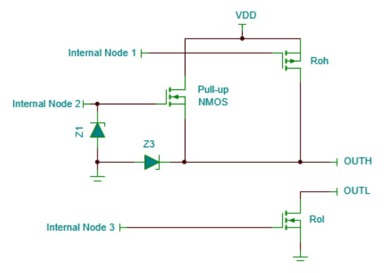
    The output stage of this device does not have zenner diode, the image below shows the output configuration of the driver.

    The body diodes of the internal MOSFETs at the stage help protect the driver from switching overshoot/undershoot.

    What are you hoping to accomplish with diode D50 on the OUTL pin?

    Also R51 and C37 are really not necessary. Are you trying to implement a filter at the gate?

    When input goes low, the driver's OUTH pin is in high impedance mode since the OUTH and OUTL are not tied together.

    Also you may want to consider increasing C38 to >=1uF as recommended in the datasheet to properly bias the driver and place it very close to the VDD pin for effective noise filter. 

    Thanks in advance for elaborating and I look forward to hearing from you.

    Regards,

    -Mamadou

  • Hi Mamadou

    Thank you for the quick answer:-)

    I use it to drive a P-channel MOSFET, and D50 is used to ensure that the MOSFET is not turned on durring startup.

    R51 and C37 is used to drive the gate without exceeding the VGS rating.(It cannot take 21V) Notice the MOSFET is turned on when UCC27538 input is low.

    C38: I have more than the 100nF on the VDD PIN, just placed elsewhere on the schematic.

    "When input goes low, the driver's OUTH pin is in high impedance mode since the OUTH and OUTL are not tied together."

    I do not think this is the case, and the reason for my question. I have looked at the datasheet and seen the principal schematic of the output stage. The problem is that OUTH is pulling down to 8V if I leave OUTL not connected.

    Can you ask the design team for more information about this output?

    Regards,

    Tune

  • Hi Tune,

    Thanks for the clarification!

    I will get back to you Monday/Tuesday.

    Thanks for your patience.

    Regards,

    -Mamadou
  • Hi Tune,

    Thanks for your patience and previous explanation of your circuit.

    I've reached out to my design and I should hear from them by the end of the week.

    In the meantime, (out of curiosity, if possible) can you share application and/or end equipment for this design?

    Also, you specified that VP=21V, VN=0V, What is VZ?

    Regarding the following subject, "When input goes low, the driver's OUTH pin is in high impedance mode since the OUTH and OUTL are not tied together."

    I will refer you to Table 5 (I/O logic truth table) of the datasheet where we specify the driver's output pins behavior:

    Thanks again for your time and patience.

    Regards,

    -Mamadou

  • Hi Mamadou

    Thank you, looking forward to their response.

    VZ is about 6V, but not important for my question.

    It is for a gatedriver driving large IGBT's.

    Regards,

    Tune

  • Thank you Tune,

    You will hear from me as soon as they get back to me.

    Thanks.

    Regards,

    -Mamadou
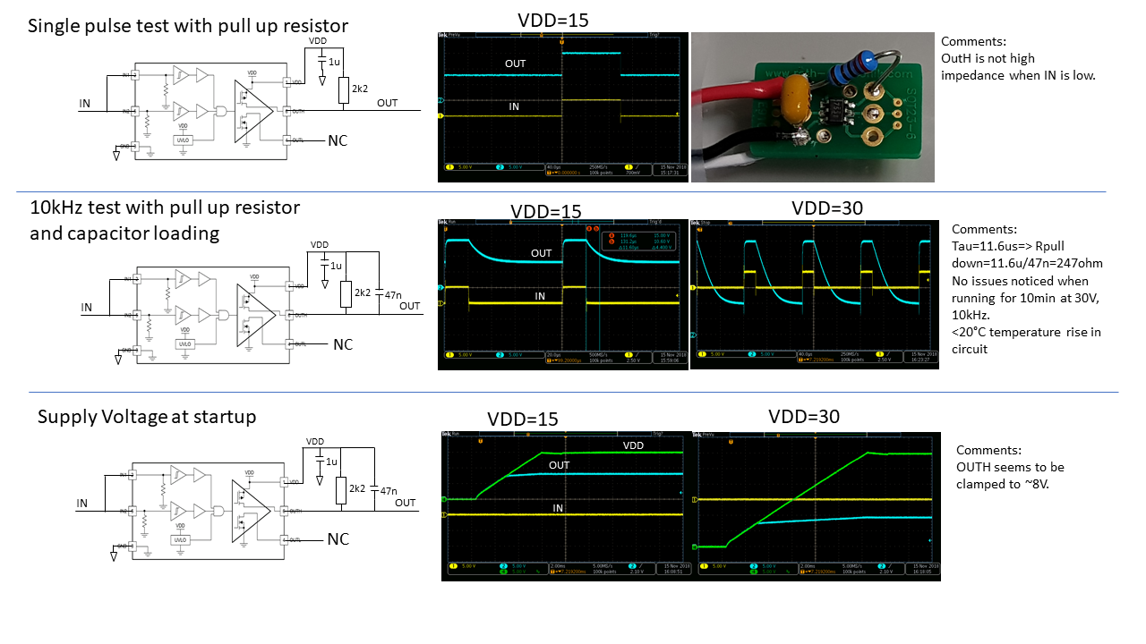
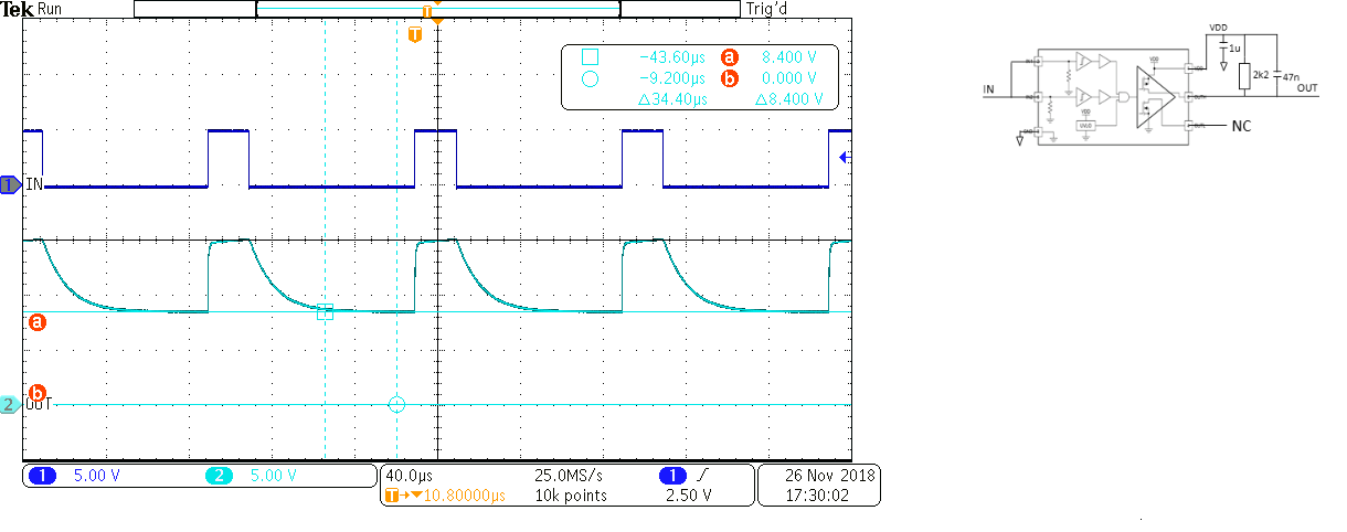
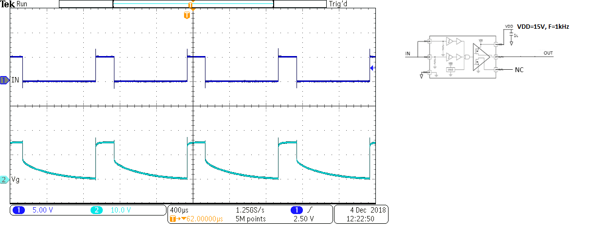
  • I have added some measurement below i just made to understand the output better. I build a small test board, and tried to keep it as simple as possible with a pull up resistor, and also tried with much more capacitive loading than what I have in the real circuit.

    I hope you can provide a more detailed diagram, than what is provided in the datasheet, and tell me if it is safe to use the device this way.

    Looking forward to your response!

    Regards,

    Tune

  • Hi Tune,

    Mamadou is out of the office, so I'll help you with this issue.

    The diagram in the data sheet is accurate.

    It seems to me that you are seeing expected behavior with the way you have the inputs configured, but maybe I don't understand what you're trying to do. Please verify the logic table in the d/s. I don't think you want to tie INH and INL together. I think you need to split them apart to get the output you're desiring.

    Take a look and let me know what you think.
  • Hi Don

    "Please verify the logic table in the d/s. I don't think you want to tie INH and INL together."

    According to the datasheet they are called IN1 and IN2 and should follow the truth table given in the datasheet. I Do not understand why I cannot tie them together.

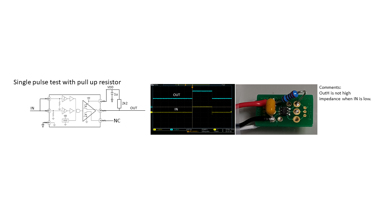
    According to this table OUTH should be high when IN1 and IN2 is high. This is also what i see when i test the device:

    When IN1 and IN2 is Low, OUTH should be high impedance according to the table. This I do not see when I test the device. Please explain to me why OUTH is ~8V when IN1 and IN2 is low. Se below test:

    Regards,

    Tune

  • Hi Tune,

    No worries! You are correct, it's fine to tie IN1 and IN2 together. I misunderstood what you were trying to do.

    In your plots is VDD at 21V?
  • Hi Don
    In this test circuit I was using VDD=15V.

    Regards,
    Tune
  • Hi Tune,

    I am an applications engineer with high power drivers and I'm here to help in Mamadou's absence.

    I have ordered samples to check this on the bench. Please give me time to receive the samples to help you on this.

    regards,
    Mateo
  • Ok, Mateo

    Looking forward to your response:-)

    Tune

  • Hello Tune, 

    Unfortunately, I did not receive samples before the holiday break.

    I will give up an update by the end of Monday 11/26. Thank you for your patience. 

    Regards,
    Mateo

  • Hi Tune,

    Thanks for your patience once again, we've received samples and I've begun testing.

    Will get back to you within 24-48hrs.

    Thanks.

    Regards,

    -Mamadou
  • Hi Tune,

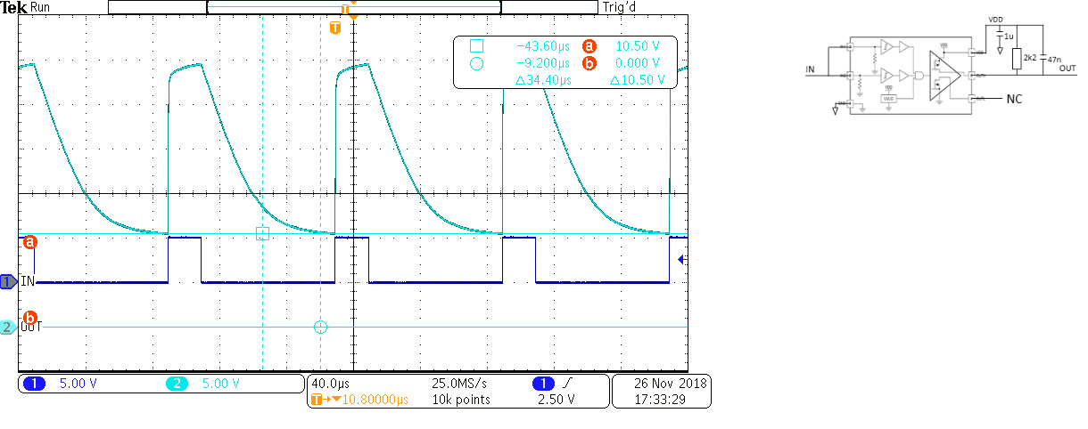
    I was able to replicate your waveforms on the bench shown below with our control units.

    There seems to be clamping at 8.2V when VDD=15V. 

    The clamping seems to go up to 10.5V at higher VDD(30V). I am still working with design to get to the bottom of it.

    I will update as soon as I get a breakthrough. 

    Thanks.

    Regards,

    -Mamadou

  • Hi Mamadou

    I cannot see your pictures, could you add them again?

    I also see the 10.5V clamping at 30V.

    Looking forward to more feedback:-)

    Regards,

    Tune

  • Hi Tune,

    Sorry about the missing images.

    My plots do confirm your observations with clamping at 8V.

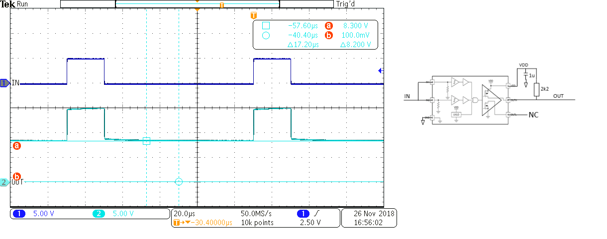
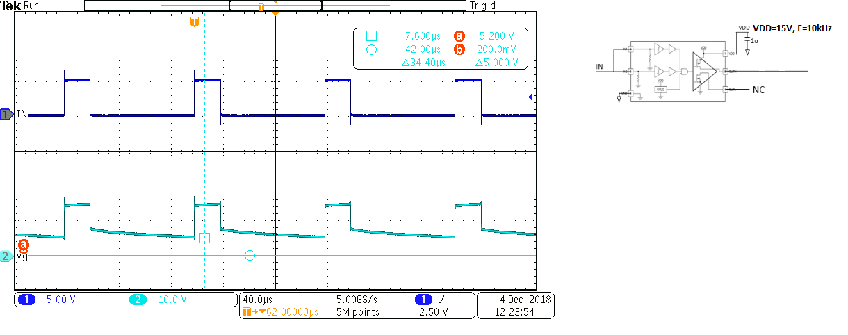
    I suspected the 2.2kOhms pullup resistor to be creating some sort of resistor divider with the internal pullup resistor which may have been the reason for the 8.2V so I removed the 2.2kohms and below were some plots at different frequencies:

    The plots still shows clamping however smaller magnitude at 5V and there seems to be a frequency dependency with 1kHz driver eventually pulling all the way down to 0V. 

  • Hi Tune,

    I am still looking into the matter with design to figure out the reason for the clamping.

    Thanks for being patient with me.

    Regards,

    -Mamadou
  • Hi Tune,

    Thanks for patiently waiting while my team and I looked into your inquiry.

    After checking with design, I can confirm the presence of an internal zener diode on the OUTH pin (to ground) to protect internal nodes. This zener diode is getting turned on from the method of operation that the device is subject to. The UCC27531 was not designed to have OUTH and OUTL separated by such a large potential.

    Based on design's feedback, I would suggest using an external zener diode (D50) capable of avalanche breakdown below 7V to protect the zener diode inside our IC.

    Please let us know if you further questions or press the green button if this addressed your concern.

    Thanks.

    Regards,

    -Mamadou
  • Yes, lets hope the design team can explain what we see...

    Thanks!

    Tune

  • Hi Mamadou

    Thank you for the feedback!

    Can you try to make a drawing on how this Zener diode is connected. If it is connected from OUTH to GND, it will be conducting large current when OUTH is high. Is it connected between OUTH and OUTL?

    It is important for my circuit that D50 has higher voltage than UCC27538's UVLO threshold, to prevent Q1 to turn on at lower voltage durring startup.(see schematic in my first post)

    Durring our testing, the device did not seem to be damaged.(Maybe it is stressed without knowing it) Can you give a rating for the internal Zener diode?

    (In out test circuit we had a 2.2kohm and a 47nF capacitor connected to the output,  without visible damage to the IC. In my circuit it is about 10kohm and ~1nF, which should stress the IC even less. It would be nice to know if this long term, will stress the IC.)

    Regards,

    Tune

  • Hi Tune,

    Sorry I wasn't very clear.

    This internal Zener diode is NOT connected between OUTH and OUTL. There is no direct connection between OUTL and OUTH.

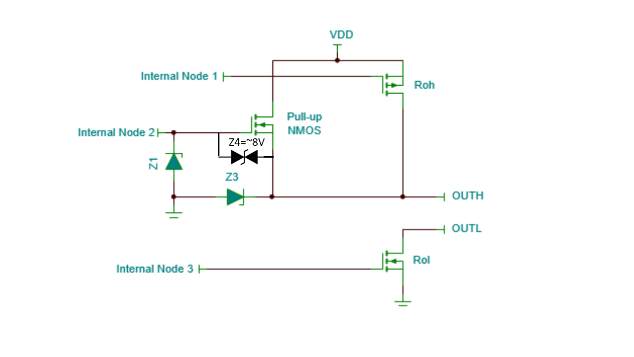
    The Zener is connected from OUTH to GND to protect the pull up NMOS of the driver. The schematic/diagram below illustrates the output structure in question. 

    So, when you command the OUTH off, the Internal Node2 is pulled to ground. This in turn causes the gate protection zeners connected gate to source to break down since you are trying to ground the OUTH, which is tied to the source. This is why we see the ~8.5V at the output. 

    The device didn't seem damaged but this mode of operation will continuously stress the pull-up N-channel FET at the risk of eventually damaging the device.

    Please consider UCC27511A as an alternative with lower UVLO (4.5V max), better timing characteristics and drive current but lower VDD range (20V abs max).

    Please let us know if you have further questions.

    Regards,

    -Mamadou

  • Hi Tune,

    To further clarify, when you command the OUTH off, Internal Node2 is pulled to ground. This in turn causes the gate protection zeners connected from gate to source to break down since you are trying to ground the OUTH, which is tied to the source. This is why we see the ~8.5V at the output.

    Please let us know if you require further assistance or press the green button if it helped address your concern.

    Regards,

    -Mamadou
  • Hi Mamadou

    You have been very helpful! I still have a few questions, that I hope you will help me with, so I do not discard my good design for no reason:-)

    Here is the schematic:

    Questions:

    1.Is it correctly understood, that it is the gate oxide in the NMOS that is stressed? What is the Vgs rating of the NMOS? (I think it is normally in the 10-20V range)
    2.When it is protected by the internal Zener will it be stressed at ~8V? (When current is limited, so the voltage is about 8-9V across the zener)
    3.Adding an external 7V zener, will that really solve the issue? (Or were this a suggestion, when you thought it was the zener diode that was the issue?)
    4.Will the internal node 2 be 0V during UVLO, so OUTH will be clamped to ~8V until VDD passes “Supply start threshold” which is specified in the datasheet to maximum 9.8V.

    Ragards,

    Tune

  • Hi Tune,

    Glad to hear back from you.

    1. Pulling INx low as currently configure is forcing the zenner to break down (connected to Vgs of NMOS) which as a result is stressing is the gate oxide of the pullup NMOS. I have not been able to confirm the internal NMOS Vgs rating.

    2. Yes there is a risk of stress even with 8V. Lower voltage (7V) should reduce this even though you have not currently observed failure during testing.  

    3. Adding an external zener would reduce the risk of damage of the internal zener whose job is to protect the pull-up NMOS. If internal zener, chances of damaging gate of the pull-up NMOS increase.

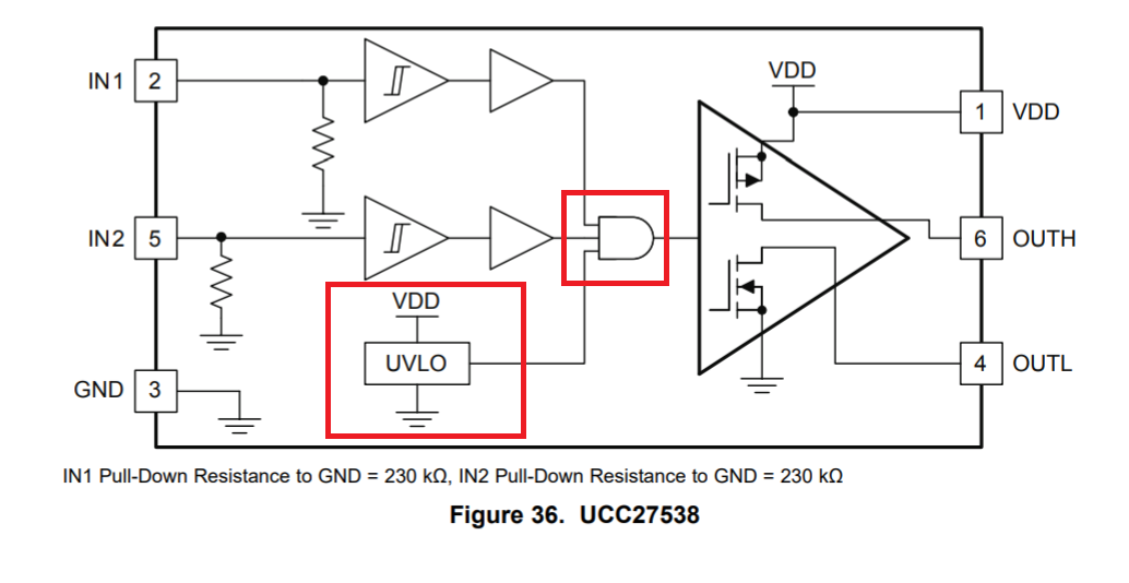
    4. Yes, internal node 2 is 0V in UVLO until there is sufficient drive voltage to activate the AND-gate (AND-gate output is essentially connected to internal node 2) shown in the functional diagram as you described:

    Please let us know if you more questions.

    Regards,

    -Mamadou