This thread has been locked.

If you have a related question, please click the "Ask a related question" button in the top right corner. The newly created question will be automatically linked to this question.

TPS7A8300: DC voltage present on output with EN pin logic low

Part Number: TPS7A8300
Other Parts Discussed in Thread: ADS54J60,

Hi,

I'm using 4 TPS7A8300s for powering an ADS54J60 on a custom board. One of the requirements for the ADS54J60 is that you bring up IOVDD (1.15V) before you bring up DRVDD (1.9VD) or else the default register values won't be loaded correctly.

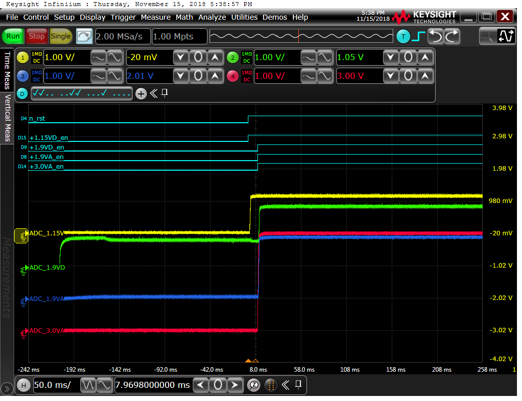
Below is a screenshot of the digital signals at the top of the screenshot in light blue, and they are driving the EN pins on each TPS7A8300 from an FPGA. The output voltages are measured at the bottom of the screenshot on Channels 1, 2, 3, & 4.

The FPGA comes out of reset (n_rst) and then sequences on the LDOs. The only problem is that the 1.9VD has about 800 mV present on the output even when it's supposed to be off.

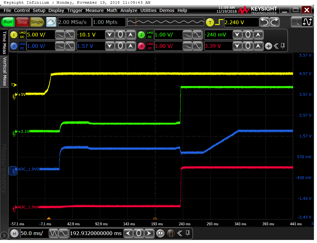
Zooming out, you can see that the 1.9VD rail comes up to 0.8V immediately on power-up, when every other rail is sitting at zero:

And my circuit for the 1.9VD:

  • Hi Charles,

    When we see situations such as this with loads which have multiple voltage rails it is usually because there is still some other rail that is up and there is leakage through the load (usually through an internal diode) to the rail that is supposed to be off. Are there any other rails that are still up during this time?

    Can you confirm a few other things for us?

    • What does the input voltage for 1.9VD look like at this time?
    • The schematics seem to show different enable signals for each LDO but I only see what appears to be one enable signat on the scope shots (1.15V). Is this the signal that is actually enabling the problem LDO?
    • How much time has elapsed from the time it was turned off and when it was turned back on?

    Sincerely,

    Kyle Van Renterghem

    Applications & Validation Manager

    Linear & Low Dropout Regulators

  • Hi Kyle,


    Are there any other rails that are still up during this time?

    Yes, the FPGA voltage rails 1V, 1.8V, 2.5V, and 3.3V are all on.

    What does the input voltage for 1.9VD look like at this time?

    Here's a screenshot of the main +5V power to the board (yellow), the intermediate 2.1V (green) which is the input to the 1.9VD, the 1.9VD (blue), and the 1.9VA (red):

    Also a block diagram of the 2.1V -> 1.9VA/1.9VD:

    The schematics seem to show different enable signals for each LDO but I only see what appears to be one enable signat on the scope shots (1.15V). Is this the signal that is actually enabling the problem LDO?


    No, there are separate enables for each LDO, it's in the screenshot here:

    How much time has elapsed from the time it was turned off and when it was turned back on?


    The time it should be powered off is during the time that 5V comes on and the FPGA asserts the enable. That's approximately 300 ms.

    One thing you might notice is that we don't see this behavior on the 1.9VA rail. The 1.9VA LDO circuit is identical to the 1.9VD. It stays at 0V until we assert the enable. I guess it comes down to the difference in the load the ADS54J60s present on 1.9VA and 1.9VD.

  • I just realized I did something in my last post that could be confusing. I changed the soft-start capacitor from 10 nF to 100 nF to see what effect that would have, but didn't change it back. Here's the same screenshot but with 10 nF soft-start:

  • Hi Charles,

    Thanks for the additional information, based on your scope shot that shows the 5V, 2.1V, and the two 1.9V rails it appears that there is an internal connection within the load (FPGA) which is causing this issue. The reason we know that the FPGA is causing this  is because the output of the LDO is actually higher than the input to the LDO. This is not how linear regulators work, other than very short transient events the output is always lower than the input voltage. This also means that you are causing reverse current to flow through the LDO to charge the input which could damage the LDO and/or reduce it's long term reliability.

    Based on the fact that the LDO output is coming up to a voltage between 1.1V and 1.4V we know that it's not coming from 1.0V rail. I'd guess it's the 1.8V rail that is charging the output of the LDO (since Vout is about a diode drop below 1.8V), but you may need to check the 2.5V and 3.3V rail as well.

    Sincerely,

    Kyle Van Renterghem

    Applications & Validation Manager

    Linear & Low Dropout Regulators

  • Kyle,

    It seems like the leakage is somehow coming through the ADC and FPGA. My hunch is that our 1.9VD rail, which is tied to pins 8 and 47 on the ADC, should be disconnected and pins 8 and 47 on the ADC should be tied to the 1.8V rail of the FPGA which is used for all the digital logic lines to/from the ADC. It looks like by using a separate supply for the ADC's digital logic, the 1.8V is leaking through to the 1.9VD output. Does that sound right? Can you share any information on the internals of the ADS54J60 that could cause that?

    I'm going to go ahead and mark this as resolved. I'd appreciate any feedback from my comments above.