


Other Parts Discussed in Thread: , TPS2121, TPS22917
Hello, I'm going to give some context first so you might understand our situation more easily
We want to design 2 different power management system with some diverse features as following:
Type A Expected features
- Automatic Switching - system must change to back-up battery automatically when main supply fails. There is no decision level, so main supply is 5v when active, or none if fails. Power supply must return to major priority power supply if it returns.
- Switchover time - As less as possible to prevent MCU reset, so seamless system is mandatory.
- Output voltage - As less as possible to prevent MCU reset. Voltage must not fall below 3v any case.
- Current Consumption – Systems works in two different stages, low current sleep mode and high-performance mode; because of that, we need good efficiency and very low Iq operating power management to not increase total sleep consumption from both power supply sources and achieve a maximum of 200 mA.
Type B. Expected features
- Automatic or manual Switching - Both options are valid
- Switchover time – A seamless system might be perfect, but breaks could be acceptable instead Instrumentation is able shutdown and restart with new power supply.
- Output voltage - As less as possible to prevent instrumentation bad function. Voltage must not fall over 4.8Vdc any case.
- Current Consumption – Power managements must achieve a maximum of 2A continuous consumptions.
In order to design a unique power management design for achieve both types (type A and B) features, we test load switches performance using TPS22916EVM following the next design (App report SLVA811A). We connect enable input to Vmain power supply with the following expected works:
When Vin1 is present: Enable is ‘1’ so Vout connect to Vin1
When Vin1 fails: Enable is ‘0’ so Vout connect to Vin2.
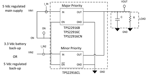
We use TPS22916CL on the minor priority power supply load switch, and we test all the others on the major priority power supply. We use both Vin2 voltages (3.3Vdc back-up battery and 5Vdc regulated power supply). We make test without load, with 10ohm load and 1Mohm load.
We have same problems regardless circuit assembly:
Once Vin1 is connected, we connect Vin2, without output load added.
We have 600nA current consumption from Vin2 -> GOOD
We have ≈33mA current consumption from Vin1 -> BAD. Unexpected
If we add an output load of 10 ohm or 1Mohm (both current type needs) we have no change on output leakage show before (these values are added to normal consumption due to load).
What could be the problem?
Once Vin1 and Vin2 are connected and Vout=Vin1. We disconnect Vin1 (Vin1 fails), then Vout = 0.5v (so it doesn’t switch to Vin2), instead of that, we have a 0.5 Vdc present on Enable pin,
What could be the source of this voltage?
We have test using a 1Mohm pull-down resistor for enable pin, but performance is the same.
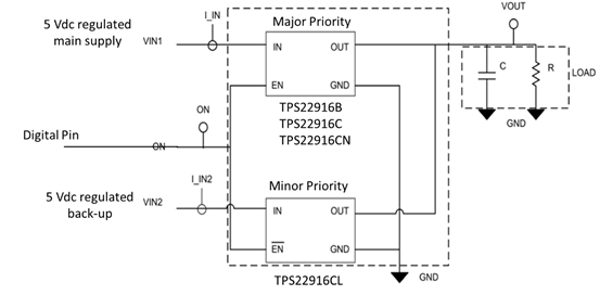
In order to design a circuit for type B requirements, we test load switches performance using TPS22916EVM following the next design (App report SLVA811A). We connect enable input to microcontroller digital output following expected works:
Enable is ‘1’ (3.3Vdc ) so Vout connect to Vin1
Enable is ‘0’ (3.3Vdc ) so Vout connect to Vin2.
We have the same current leakage problems show before, in addition with an unexpected voltage drop when we use a 5ohm load (≈1A current output).
Enable is ‘1’ so Vout connect to Vin1, and Vout falls to 4.6 Vdc. BAD. Unexpected
Enable is ‘0’ so Vout connect to Vin2, and Vout falls to 4.9 Vdc. GOOD.
What could be causing this voltage drop?
Thank you in advance!


