This thread has been locked.

If you have a related question, please click the "Ask a related question" button in the top right corner. The newly created question will be automatically linked to this question.

LM5109: Abnormal after Power Voltage Drop Test

Part Number: LM5109
Other Parts Discussed in Thread: LMR14006, , UCC27282

Hi, Team

My automotive customer is using LM5109B-Q1 in their automotive wireless charger product. They use LMR14006 to convert BATT 12V to 8.3V to VDD pin of LM5109B-Q1.

Customer conduct Power Voltage Drop test on BATT 12V input to system.  When the test is conducted, the BATT 12V will drop to 0V with different frequency. The test will last for about 1 minute. Customer require the system should be work correctly after the test, but LM5109B-Q1 can not.

There are HI and LI signal input during the test. After the Power Voltage Drop Test, the LM5109B-Q1 HO and LO output signal duty cycle is smaller than input signal on HI and LI pin respectively. Only power down and power up the LM5109B-Q1 can make it work correctly.

If customer replace LM5109B-Q1 to IR2301, the test is pass.

Is there any suggestion on this issue?

Here is customer shcematic:

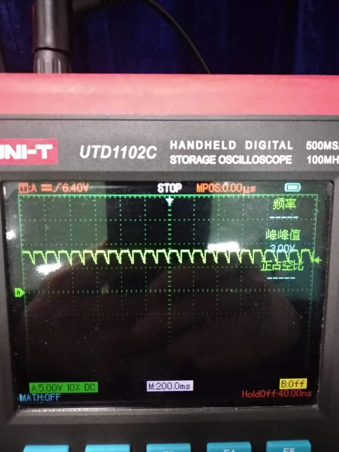
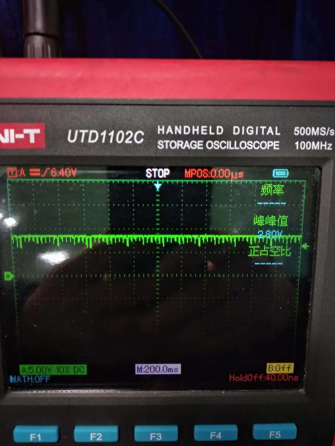
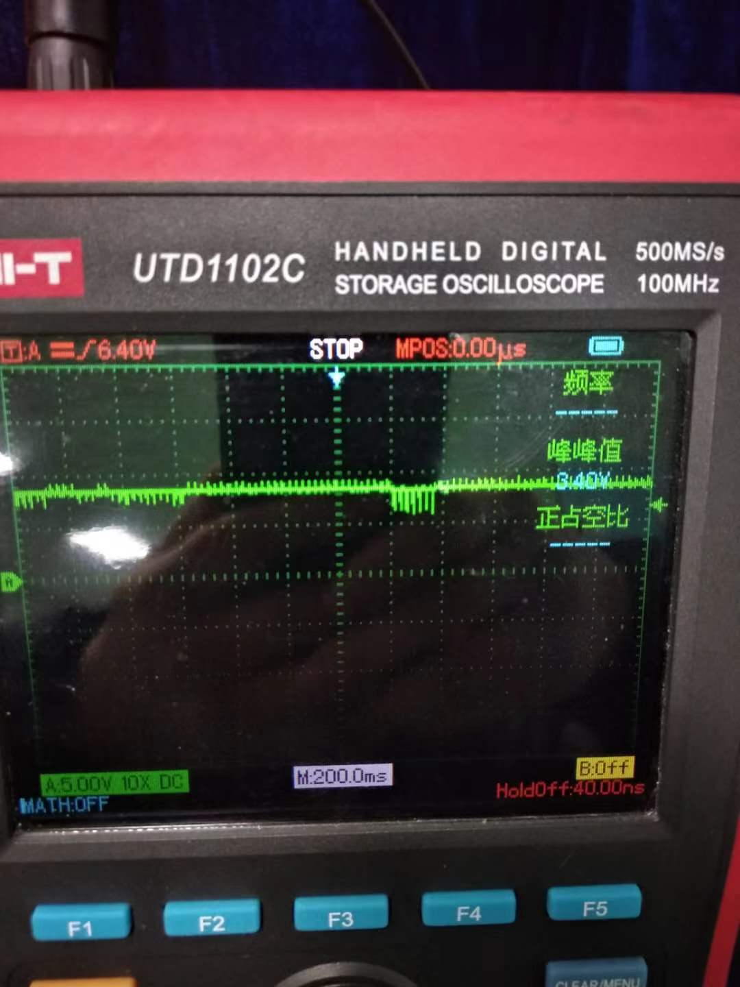
Here is hte waveform of BATT 12V.

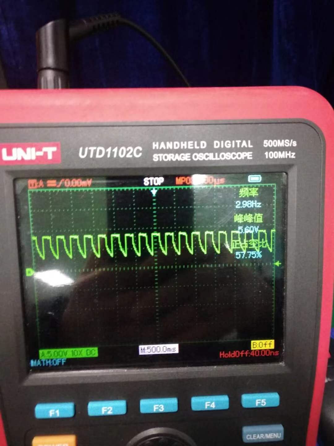
Here is the waveform on VDD pin during the test. The VDD voltage will drop to as low as 3V.

Thanks

Kevin

  • Hello Kevin,
    Thank you for the interest in the LM5109B-Q1. I need to get some more details on the test and conditions to be able to provide information to help resolve the concern.
    On the scope plots, is the waveform one of the outputs, either LO and HO, curing the progression of the VBATT voltage cycling? I assume that is the case.
    During the Vbatt cycling to 0V, is the LI and HI inputs always active signals? Is LI and HI high when LM5109B-Q1 VDD is at 0V?
    What is the frequency, duty cycle and amplitude of LI and HI? What is the frequency, rising and falling time of VBATT during the power cycling test?
    It would help to have scope plots of LI and HI with LO and HO showing the progression of incorrect duty cycle. Also the LM5109B VDD and LI and HI plots will be helpful.
    Regards
    Richard Herring
  • Hi, Richard

    1. The first video in my last post is the waveform of VBATT voltage cycling.

    2. During the VBATT voltage cycling to 0V, the LI and HI input keep active.

    3.The frequency of HI and LI is 200kHz, and the duty cycle keep changing.

    4. Please refer to the first video in my last post for the frequency, rising and falling time of VBATT during the power cycling test.

    5. Plesae refer to the last 3 figures in my last post for the waveform of LM5109B-Q1 VDD pin during the power cycling test.

    6. Customer will measure LI, HI, LO, HO at the same time soon.

    Please help to check the cause. Is there any suggestion to solve the issue?

    As VDD pin will drop to 3V during the test, it will keep triggering UVLO of LM5109B-Q1. Is it better to choose a part with lower UVLO? Is there any better part suggested?

    Thanks

    Kevin

  • Hello Kevin,

    Thank you for the clarification on the waveforms in the video, and the following waveforms. Can you confirm if 3V is the lowest level that you see on the LM5109B VDD during the test? The UVLO will be triggered in this condition, and the LO and HO outputs will not be active.

    There are a couple of things to consider, and try regarding the VDD drop. There is a newer 100V half bridge driver with lower UVLO that may help, although the UVLO is ~5V, not 3V. The UCC27282 is an option that may help, the datasheet can be found here:

    Also you can try increasing the capacitance on the LM5109B VDD, C80 to prevent VDD from dropping to the UVLO shutdown during the test. It may take at least 33uF (Vs 10uF) to help hold up VDD.

    I can take a look at the basic behavior of the IC with constant LI and HI, with VDD voltage droops, but will not be able to duplicate your power converter. Consider if the UCC27282 may be an option, and try the increased VDD capacitance.

    Regards,

    Richard Herring