This thread has been locked.

If you have a related question, please click the "Ask a related question" button in the top right corner. The newly created question will be automatically linked to this question.

CCS/UCD3138A64: CCS/UCD3138A64:

Part Number: UCD3138A64
Other Parts Discussed in Thread: UCD3138, UCD3138064

Tool/software: Code Composer Studio

Good Morning , 

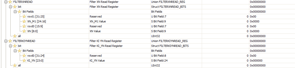
I want to drive an LLC . In this app , I want to vary the input of the filter using CPU sample  and as a result   I generate two DPWMs  in resonant mode with variable frequency.

Here My code.

It's doesn't work

Please Help!!!

Thank you 

//###########################################################################
//
// FILE: main.c
//
// TITLE: main
//
// NOTES:
// 1)

//###########################################################################
//
// Ver | dd mmm yyyy | Who | Description of changes
// ======|=============|======|==============================================
// 1.00 | 05 May 2015 | CH |
//
// Texas Instruments, Inc
// Copyright Texas Instruments 2008. All rights reserved.
//###########################################################################
#define MAIN 1

#include "system_defines.h"
#include "Cyclone_Device.h"
#include "pmbus_commands.h"
#include "pmbus_common.h"
#include "pmbus_topology.h"
#include "variables.h"
#include "functions.h"
#include "software_interrupts.h"
#include "cyclone_defines.h"
#include "stdio.h"

#define PCLK_PERIOD 4.0e-9 // Time base in seconds
#define PERIOD_SECONDS 2.22e-6 // fmax = 450 KHZ
#define RETARD_SECONDS 100e-9 // config temps mort

#define PERIOD ((int)(PERIOD_SECONDS/PCLK_PERIOD)<<4) // (starting from bit 4)
#define RETARD ((int)(RETARD_SECONDS/PCLK_PERIOD)<<4) // (starting from bit 4)
#define EVENT1 (int)(PERIOD*0.00)
#define EVENT2 (int)(PERIOD*0.50)
#define EVENT3 (int)(PERIOD*0.50)
#define EVENT4 (int)(PERIOD*0.00)

int input_filtre ;// comment for hyperknob [min=0, max=1200, step=100]

/*****************Configuration DPWM******************************/

void init_dpwm0(void)
{


Dpwm0Regs.DPWMCTRL0.bit.PWM_EN = 1; // PWM_EN – PWM Processing Enable
//0 = Disable PWM module, outputs zero (Default)
// 1 = Enable PWM operationy

Dpwm0Regs.DPWMCTRL0.bit.CLA_EN = 1; // CLA Processing Enable
//0 = Generate PWM waveforms from PWM Register values (Default)
//1 = Enable CLA input


Dpwm0Regs.DPWMSAMPTRIG1.all = PERIOD ; //3/4 of period
Dpwm0Regs.DPWMCTRL2.bit.SAMPLE_TRIG_1_EN = 1; //enable 1 sample trigger


//Resonant Mode
Dpwm0Regs.DPWMCTRL0.bit.PWM_MODE = 1; //DPWM Mode
// 0 = Normal Mode
// 1 = Resonant Mode
// 2 = Multi-Output Mode
// 3 = Triangular Mode
// 4 = Leading Mode

Dpwm0Regs.DPWMCTRL0.bit.RESON_MODE_FIXED_DUTY_EN =0; //Configures how duty cycle is controlled in Resonance Mode
//0 = Resonant mode duty cycle set by Filter duty (Default)
// 1 = Resonant mode duty cycle set by Auto Switch High Register

Dpwm0Regs.DPWMCTRL0.bit.CBC_ADV_CNT_EN =0 ; //Selects cycle-by-cycle of operation
// Normal Mode
// 0 = CBC disabled (Default)
// 1 = CBC enabled
// Multi and Resonant Modes
// 0 = PWM-A and PWM-B operate independently (Default)
// 1 = PWM-A and PWM-B pulse matching enabled


Dpwm0Regs.DPWMCTRL1.bit.HIRES_DIS = 0; //0 = Enable High Resolution logic


Dpwm0Regs.DPWMCTRL1.bit.CHECK_OVERRIDE = 1; //Disable math checks, there is a bug in the hardware

Dpwm0Regs.DPWMCTRL1.bit.EVENT_UP_SEL = 1; // Update End Period Mode
// 0 = Events updated anytime (Default)
// 1 = Events updated at End of Period

Dpwm0Regs.DPWMCTRL2.bit.FILTER_DUTY_SEL = 2; //– Sets which register is used for the max duty calculation at the
// Filter in RESON and MESH modes.
// 0 = PWM Period Register (Default)
// 1 = Event 2
// 2 = PWM Period Adjust Register (Bits 13:0)


Dpwm0Regs.DPWMPHASETRIG.bit.PHASE_TRIGGER = 2; // Phase Trigger = Phase Trigger Register value or Filter Duty

Dpwm0Regs.DPWMCTRL1.bit.GLOBAL_PERIOD_EN = 1;

Dpwm0Regs.DPWMCTRL0.bit.MSYNC_SLAVE_EN = 0; //0 = PWM not synchronized to another PWM channel
LoopMuxRegs.DPWMMUX.bit.DPWM0_SYNC_SEL = 0; //0 = DPWM0 with DPWM0 Sync
Dpwm0Regs.DPWMPHASETRIG.all = 32; //128ns phase delay


Dpwm0Regs.DPWMEV1.all = EVENT1; // set EVENT 1 to 0% (start) of period
Dpwm0Regs.DPWMEV2.all = EVENT2; // set EVENT 2 to 25% of period
Dpwm0Regs.DPWMEV3.all = EVENT3; // set EVENT 3 to 50% of period
Dpwm0Regs.DPWMEV4.all = EVENT4; // set EVENT 4 to 75% of period

Dpwm0Regs.DPWMPRD.all = PERIOD; // use .all for all values, so that the scaling matches


Dpwm0Regs.DPWMRESDUTY.bit.RESONANT_DUTY=(PERIOD+1)>>1 ; // Controls the DPWM duty. 16-bit signed number is used
// as a Filter Output Multiplier in Resonant Mode.

Dpwm0Regs.DPWMCTRL0.bit.MIN_DUTY_MODE = 0;

// Dpwm0Regs.DPWMCTRL0.bit.CBC_PWM_AB_EN =1 ; //Sets if Fault CBC changes output waveform for PWM-A and PWMB
//0 = PWM-A and PWM-B unaffected by Fault CBC (Default)
//1 = PWM-A and PWM-B affected by Fault CBC

//Dpwm0Regs.DPWMCTRL1.bit.CBC_BSIDE_ACTIVE_EN =1 ; ///Sets if CBC responds to Fault CBC when PWM-B is active,
// only available in Multi and Reson modes
// 0 = Response to Fault CBC when PWM-A active (Default)
// 1 = Response to Fault CBC when PWM-A or PWM-B active

}

void init_filter0(void)
{
// special set up for CPU SAMPLE - all coefficients are zeroed except for P.
Filter0Regs.FILTERCTRL.bit.USE_CPU_SAMPLE = 1; // enable CPU Sample

Filter0Regs.CPUXN.bit.CPU_SAMPLE = 64; // set to 1/4
Filter0Regs.FILTERKPCOEF0.bit.KP_COEF_0=1; //full pass through of XN value.
Filter0Regs.FILTERKICOEF0.bit.KI_COEF_0=1;
Filter0Regs.FILTERKDCOEF0.bit.KD_COEF_0=0;
Filter0Regs.FILTERKDALPHA.bit.KD_ALPHA_0=-1;
Filter0Regs.FILTERKICLPHI.bit.KI_CLAMP_HIGH = 0x7FFFFF;
Filter0Regs.FILTERKICLPLO.bit.KI_CLAMP_LOW = 0;

Filter0Regs.FILTEROCLPHI.bit.OUTPUT_CLAMP_HIGH = 0x7FFFFF;
Filter0Regs.FILTEROCLPLO.bit.OUTPUT_CLAMP_LOW = 0;

Filter0Regs.FILTERCTRL.bit.OUTPUT_MULT_SEL = 3; //Selects output multiplicand used for multiplying with
// filter output to calculate DPWM Duty value
// 0 = KComp received from Loop Mux module (Default)
// 1 = Switching period received from Loop Mux module
// 2 = Feed-Forward value received from Loop Mux module
// 3 = Resonant Duty value received from DPWM Module


Filter0Regs.FILTERCTRL.bit.PERIOD_MULT_SEL = 1; //Selects output multiplicand used for multiplying with filter output
// to calculate DPWM Period value in Resonant Mode
// 0 = Switching period received from Loop Mux module (Default)
// 1 = KComp received from Loop Mux module
Filter0Regs.FILTERCTRL.bit.OUTPUT_SCALE = 0; /// no shift
Filter0Regs.FILTERCTRL.bit.FILTER_EN = 1;

}

void init_loop_mux(void)
{

LoopMuxRegs.SAMPTRIGCTRL.bit.FE0_TRIG_DPWM0_EN = 1; // use DPWM0 for filter0 sample trigger

//DPWM-0 connects to filter for resonant duty

LoopMuxRegs.FILTERMUX.bit.FILTER0_PER_SEL = 0; // Selects source of switching cycle period for Filter 0
//Module
//0 = DPWM 0 Switching Period (Default)
//1 = DPWM 1 Switching Period
//2 = DPWM 2 Switching Period
LoopMuxRegs.FILTERKCOMPA.bit.KCOMP0 =PERIOD ; //3 = DPWM 3 Switching Period
//Use value in KCOMP-0 register
LoopMuxRegs.FILTERMUX.bit.FILTER0_KCOMP_SEL = 0;


//Connect FILTER-0 to DPWM-0

LoopMuxRegs.DPWMMUX.bit.DPWM0_FILTER_SEL = 0; // Selects source of duty cycle/resonant period for
//DPWM Module 0
//0 = Filter 0 Output Selected (Default)
//1 = Filter 1 Output Selected
//2 = Filter 2 Output Selected
//3 = Constant Power Module Selected
//4 = DPWM_ON_TIME value from Light Load Control Register
LoopMuxRegs.LLENTHRESH.bit.CYCLE_CNT_THRESH = 0; //

}

void global_enable(void)
{
union GLBEN_REG glben_store; // collect global enable bits for simultaneous use
glben_store.all = 0;
glben_store.bit.DPWM0_EN = 1;
glben_store.bit.FE_CTRL0_EN = 1;
LoopMuxRegs.GLBEN = glben_store;
}

void main()
{
// enable JTAG
MiscAnalogRegs.IOMUX.all = 0;

//---------------------------------------------------------------------------
// IMPORTANT: READ BELOW, OR CODE MAY NOT EXECUTE CORRECTLY
//---------------------------------------------------------------------------
// tie pin FAULT3 to ground for normal operation
// tie pin FAULT3 to 3.3V to clear checksum
if(GioRegs.FAULTIN.bit.FLT3_IN == 0)
{
clear_integrity_word();
}

#if (UCD3138|UCD3138064)
MiscAnalogRegs.CLKTRIM.bit.HFO_LN_FILTER_EN = 0;
MiscAnalogRegs.CSTRIM.bit.RESISTOR_TRIM =23; //28;
#endif


input_filtre= Filter0Regs.CPUXN.bit.CPU_SAMPLE; // initialize hyperknob

init_dpwm0();
init_filter0();
init_loop_mux();
init_pmbus(0x58);
global_enable();


for(;;)
{
pmbus_handler();
Filter0Regs.CPUXN.bit.CPU_SAMPLE = input_filtre; // put hyperknob value into register
}
}


//#pragma INTERRUPT(c_int00,RESET)

void c_int00(void)
{
main();
}

  • Have you tried to debug your code using memory debugger and see how the digital signal propagates through the filter and DPWM?
    It is hard for me to debug the code just by looking at it, but the statement:
    LoopMuxRegs.FILTERKCOMPA.bit.KCOMP0 =PERIOD; looks suspicious. Please note that the KCOMP0 and the DPWM's PRD are not the of the same resolution.
  • Thank  u for ur prompt reply, Sir.

    I correct my mistake about the Kcomp.

    Yeah I verified with the memory debugger and the problem is that   the input of the filter XN and the output  of the filter are equals to zero even if I change the  input of the  filter  using CPU sample

    My strategy is to  put the period in the kcomp of the  PERIOD_MULT_SEL and  fix the resonant e in OUTPUT_MULT_SEL and to change the frequency I found this in that I should use the global period PWM and KCOMP to change

    it  

    I added this line code to the previous one but I got nothing I'll appreaciate ur advices. Thanks a lot I'am blocked 

    if (input_filtre2>input_filtre1)
    {
    LoopMuxRegs.PWMGLBPER.all= PERIOD;
    _wait(8800) ;
    LoopMuxRegs.FILTERKCOMPA.bit.KCOMP0 =(PERIOD) >> 4; // KCOMP is at 4 ns, period is at 250 ps//Use value in KCOMP-0 register
    }


    else
    {
    LoopMuxRegs.FILTERKCOMPA.bit.KCOMP0 =(PERIOD) >> 4; // KCOMP is at 4 ns, period is at 250 ps//Use value in KCOMP-0 register
    _wait(8800) ;
    LoopMuxRegs.PWMGLBPER.all= PERIOD;

    }

    //###########################################################################
    //
    // FILE: main.c
    //
    // TITLE: main
    //
    // NOTES:
    // 1)

    //###########################################################################
    //
    // Ver | dd mmm yyyy | Who | Description of changes
    // ======|=============|======|==============================================
    // 1.00 | 05 May 2015 | CH |
    //
    // Texas Instruments, Inc
    // Copyright Texas Instruments 2008. All rights reserved.
    //###########################################################################
    #define MAIN 1

    #include "system_defines.h"
    #include "Cyclone_Device.h"
    #include "pmbus_commands.h"
    #include "pmbus_common.h"
    #include "pmbus_topology.h"
    #include "variables.h"
    #include "functions.h"
    #include "software_interrupts.h"
    #include "cyclone_defines.h"
    #include "stdio.h"

    #define PCLK_PERIOD 4.0e-9 // Time base in seconds 4ns
    #define PERIOD_SECONDS 2.22e-6 // fmax = 450 KHZ
    #define RETARD_SECONDS 100e-9 // config temps mort

    #define PERIOD ((int)(PERIOD_SECONDS/PCLK_PERIOD)<<4) // (starting from bit 4)
    #define RETARD ((int)(RETARD_SECONDS/PCLK_PERIOD)<<4) // (starting from bit 4)
    #define EVENT1 (int)(PERIOD*0.00)
    #define EVENT2 (int)(PERIOD*0.50)
    #define EVENT3 (int)(PERIOD*0.50)
    #define EVENT4 (int)(PERIOD*0.00)


    #define PWM_MODE_ON (0)
    int input_filtre ;// comment for hyperknob [min=0, max=300, step=1]
    int input_filtre1;
    int input_filtre2;

    /****************************************************************/
    void _wait( int delay )
    {
    int i;
    for( i = 0 ; i < delay ; i++ ){}
    }
    /****************************************************************/

    /*****************Configuration DPWM******************************/

    void init_dpwm0(void)
    {


    Dpwm0Regs.DPWMCTRL0.bit.CLA_EN = 1; // CLA Processing Enable
    //0 = Generate PWM waveforms from PWM Register values (Default)
    //1 = Enable CLA input
    Dpwm0Regs.DPWMSAMPTRIG1.all = PERIOD ;
    Dpwm0Regs.DPWMCTRL2.bit.SAMPLE_TRIG_1_EN = 1; //enable 1 sample trigger


    //DPWM Mode
    // 0 = Normal Mode
    // 1 = Resonant Mode
    // 2 = Multi-Output Mode
    // 3 = Triangular Mode
    // 4 = Leading Mode

    Dpwm0Regs.DPWMCTRL0.bit.PWM_MODE = 1; //Resonant Mode

    Dpwm0Regs.DPWMCTRL0.bit.RESON_MODE_FIXED_DUTY_EN =0; //Configures how duty cycle is controlled in Resonance Mode
    //0 = Resonant mode duty cycle set by Filter duty (Default)
    // 1 = Resonant mode duty cycle set by Auto Switch High Register
    Dpwm0Regs.DPWMCTRL0.bit.CBC_ADV_CNT_EN =0 ; //Selects cycle-by-cycle of operation
    // Normal Mode
    // 0 = CBC disabled (Default)
    // 1 = CBC enabled
    // Multi and Resonant Modes
    // 0 = PWM-A and PWM-B operate independently (Default)
    // 1 = PWM-A and PWM-B pulse matching enabled
    Dpwm0Regs.DPWMCTRL1.bit.HIRES_DIS = 0; //0 = Enable High Resolution logic
    Dpwm0Regs.DPWMCTRL1.bit.CHECK_OVERRIDE = 1; //Disable math checks, there is a bug in the hardware
    Dpwm0Regs.DPWMCTRL1.bit.EVENT_UP_SEL = 1; // Update End Period Mode
    // 0 = Events updated anytime (Default)
    // 1 = Events updated at End of Period
    Dpwm0Regs.DPWMCTRL2.bit.FILTER_DUTY_SEL = 2; //– Sets which register is used for the max duty calculation at the
    // Filter in RESON and MESH modes.
    // 0 = PWM Period Register (Default)
    // 1 = Event 2
    // 2 = PWM Period Adjust Register (Bits 13:0)
    Dpwm0Regs.DPWMPHASETRIG.bit.PHASE_TRIGGER = 2; // Phase Trigger = Phase Trigger Register value or Filter Duty
    Dpwm0Regs.DPWMCTRL1.bit.GLOBAL_PERIOD_EN = 1;
    Dpwm0Regs.DPWMCTRL0.bit.MSYNC_SLAVE_EN = 0; //0 = PWM not synchronized to another PWM channel
    LoopMuxRegs.DPWMMUX.bit.DPWM0_SYNC_SEL = 0; //0 = DPWM0 with DPWM0 Sync
    Dpwm0Regs.DPWMPHASETRIG.all = 32; //128ns phase delay


    Dpwm0Regs.DPWMEV1.all = EVENT1; // set EVENT 1 to 0% (start) of period
    Dpwm0Regs.DPWMEV2.all = EVENT2; // set EVENT 2 to 50% of period
    Dpwm0Regs.DPWMEV3.all = EVENT3; // set EVENT 3 to 50% of period
    Dpwm0Regs.DPWMEV4.all = EVENT4; // set EVENT 4 to 75% of period
    Dpwm0Regs.DPWMPRD.all = PERIOD; // use .all for all values, so that the scaling matches
    Dpwm0Regs.DPWMRESDUTY.bit.RESONANT_DUTY=(((PERIOD/2) >> 4)+1)>>1 ; // Controls the DPWM duty. 16-bit signed number is used
    // as a Filter Output Multiplier in Resonant Mode.
    Dpwm0Regs.DPWMCTRL0.bit.MIN_DUTY_MODE = 0;
    Dpwm0Regs.DPWMCTRL0.bit.CBC_PWM_AB_EN =1 ; //Sets if Fault CBC changes output waveform for PWM-A and PWMB
    //0 = PWM-A and PWM-B unaffected by Fault CBC (Default)
    //1 = PWM-A and PWM-B affected by Fault CBC
    Dpwm0Regs.DPWMCTRL1.bit.CBC_BSIDE_ACTIVE_EN =1 ; ///Sets if CBC responds to Fault CBC when PWM-B is active,
    // only available in Multi and Reson modes
    // 0 = Response to Fault CBC when PWM-A active (Default)
    // 1 = Response to Fault CBC when PWM-A or PWM-B active
    Dpwm0Regs.DPWMCTRL1.bit.GLOBAL_PERIOD_EN=1 ; //
    Dpwm0Regs.DPWMCTRL0.bit.PWM_EN = 1; // PWM_EN – PWM Processing Enable
    //0 = Disable PWM module, outputs zero (Default)

    // 1 = Enable PWM operationy
    }

    void init_filter0(void)
    {

    Filter0Regs.FILTERCTRL.bit.USE_CPU_SAMPLE = 1; // enable CPU Sample
    Filter0Regs.CPUXN.bit.CPU_SAMPLE = 64; // set to 1/4
    Filter0Regs.FILTERKPCOEF0.bit.KP_COEF_0; //full pass through of XN value.
    Filter0Regs.FILTERKICOEF0.bit.KI_COEF_0;
    Filter0Regs.FILTERKDCOEF0.bit.KD_COEF_0;
    Filter0Regs.FILTERKDALPHA.bit.KD_ALPHA_0;
    Filter0Regs.FILTERCTRL.bit.OUTPUT_MULT_SEL = 3; //Selects output multiplicand used for multiplying with
    // filter output to calculate DPWM Duty value
    // 0 = KComp received from Loop Mux module (Default)
    // 1 = Switching period received from Loop Mux module
    // 2 = Feed-Forward value received from Loop Mux module
    // 3 = Resonant Duty value received from DPWM Module
    Filter0Regs.FILTERCTRL.bit.PERIOD_MULT_SEL = 1; //Selects output multiplicand used for multiplying with filter output
    // to calculate DPWM Period value in Resonant Mode
    // 0 = Switching period received from Loop Mux module (Default)
    // 1 = KComp received from Loop Mux module
    Filter0Regs.FILTERCTRL.bit.OUTPUT_SCALE = 0; /// no shift
    Filter0Regs.FILTERCTRL.bit.FILTER_EN = 1;
    }

    void init_loop_mux(void)

    {


    LoopMuxRegs.SAMPTRIGCTRL.bit.FE0_TRIG_DPWM0_EN = 1; // use DPWM0 for filter0 sample trigger
    LoopMuxRegs.FILTERMUX.bit.FILTER0_PER_SEL = 0; // Selects source of switching cycle period for Filter 0
    //Module
    //0 = DPWM 0 Switching Period (Default)
    //1 = DPWM 1 Switching Period
    //2 = DPWM 2 Switching Period
    //3 = DPWM 3 Switching Period
    LoopMuxRegs.FILTERMUX.bit.FILTER0_KCOMP_SEL = 0;

    LoopMuxRegs.DPWMMUX.bit.DPWM0_FILTER_SEL = 0; // Selects source of duty cycle/resonant period for
    //DPWM Module 0
    //0 = Filter 0 Output Selected (Default)
    //1 = Filter 1 Output Selected
    //2 = Filter 2 Output Selected
    //3 = Constant Power Module Selected
    //4 = DPWM_ON_TIME value from Light Load Control Register

    //. It is also used to match up the PWM and Resonant mode waveforms in the LLC configuration.

    LoopMuxRegs.FILTERKCOMPA.bit.KCOMP0 =(PERIOD) >> 4; // KCOMP is at 4 ns, period is at 250 ps//Use value in KCOMP-0 register

    /*If the Global Period Enable (GLOBAL_PERIOD_EN) bit is set in DPWMCTRL1 of a DPWM
    module, it will use the value in PWMGLBPRD for its period. This can be used to change the
    periods of multiple DPWMs with one C statement. This is useful for frequency dithering. Note
    that the period change takes effect at the end of the previous period. If DPWMs are out of phase,
    the frequency change will take place at a different time for each DPWM.
    Also note that the if the Filter is using the Period from the DPWM for calculations, it will still use
    the DPWM Period Register even if the Global Period is enabled. So to use the Global Period, it is
    necessary to use the KCOMP register as a multiplier and to change both the Global Period
    Register and the KCOMP register at the same time. In fact, a careful sequence should be
    followed:
    If the period is increasing – first change the Global Period Register, then wait 1 period, then
    change the KCOMP. This sequence guards against dead time violations.
    For the same reason, when decreasing the period, change the KCOMP first.
    For any frequency change, the order of changes should be carefully designed based on the
    actual topology and IC configuration.*/

    LoopMuxRegs.PWMGLBPER.all= PERIOD;


    LoopMuxRegs.LLENTHRESH.bit.CYCLE_CNT_THRESH = 0; //
    }

    void global_enable(void)
    {
    union GLBEN_REG glben_store; // collect global enable bits for simultaneous use
    glben_store.all = 0;
    glben_store.bit.DPWM0_EN = 1;
    glben_store.bit.FE_CTRL0_EN = 1;
    LoopMuxRegs.GLBEN = glben_store;
    }

    void main()
    {
    // enable JTAG
    MiscAnalogRegs.IOMUX.all = 0;

    //---------------------------------------------------------------------------
    // IMPORTANT: READ BELOW, OR CODE MAY NOT EXECUTE CORRECTLY
    //---------------------------------------------------------------------------
    // tie pin FAULT3 to ground for normal operation
    // tie pin FAULT3 to 3.3V to clear checksum
    if(GioRegs.FAULTIN.bit.FLT3_IN == 0)
    {
    clear_integrity_word();
    }

    #if (UCD3138|UCD3138064)
    MiscAnalogRegs.CLKTRIM.bit.HFO_LN_FILTER_EN = 0;
    MiscAnalogRegs.CSTRIM.bit.RESISTOR_TRIM =23; //28;
    #endif


    input_filtre= Filter0Regs.CPUXN.bit.CPU_SAMPLE; // initialize hyperknob
    input_filtre1=input_filtre ;

    init_filter0();
    init_loop_mux();
    init_dpwm0();
    init_pmbus(0x58);
    global_enable();


    for(;;)
    {
    pmbus_handler();
    Filter0Regs.CPUXN.bit.CPU_SAMPLE = input_filtre; // put hyperknob value into register
    // input_filtre2=input_filtre ;
    }
    /* if (input_filtre2>input_filtre1)
    {
    LoopMuxRegs.PWMGLBPER.all= PERIOD;
    _wait(8800) ;
    LoopMuxRegs.FILTERKCOMPA.bit.KCOMP0 =(PERIOD) >> 4; // KCOMP is at 4 ns, period is at 250 ps//Use value in KCOMP-0 register
    }


    else
    {
    LoopMuxRegs.FILTERKCOMPA.bit.KCOMP0 =(PERIOD) >> 4; // KCOMP is at 4 ns, period is at 250 ps//Use value in KCOMP-0 register
    _wait(8800) ;
    LoopMuxRegs.PWMGLBPER.all= PERIOD;

    }*/
    }


    //#pragma INTERRUPT(c_int00,RESET)

    void c_int00(void)
    {
    main();
    }

  • Seems like your FE0 (and Filter0) are not getting triggered by DPWM0.

    Please replace the statement:

    Dpwm0Regs.DPWMSAMPTRIG1.all = PERIOD ;

    With:

    Dpwm0Regs.DPWMSAMPTRIG1.all = 256; // 64 nS after the beginning


    This should help to run the filter.
    Alternatively you could periodically set the bit FORCE_START in the FILTERCTRL register.

    Regards,

  • I'am sorry if I bothered u by my questions.
    In fact, I don't use a front end just my goal is to change the iunput of the filter and as a consequence the DPWM in a resonant mode will change .
    Later, if this step is validated i will integrate the front end and the autoswitch mecanism .
    My problem that with normal mode the CPU sample it's okay I mean if i change the input_filtre the FILTERXNREADER change proportionnally and as a result the duty cycle change.But here with resonant mode I didn't understand why I have zero fro FILTERXNREADER register when I change the CPU SAMPLE variable .
    I took ur advise and I changed what u said to me but still doesn't work :( .

    Dpwm0Regs.DPWMSAMPTRIG1.all = PERIOD - 2000 ; // 500 nS before the end of period

    And this

    Filter0Regs.FILTERCTRL.bit.FORCE_START = 1; // Initiates a filter calculation under firmware control
    // 0 = No calculation started (Default)
    // 1 = Calculation started


    AM sorry if i talked too much but Iam blocked .
    Thank u for ur help .


    //###########################################################################
    //
    // FILE: main.c
    //
    // TITLE: main
    //
    // NOTES:
    // 1)

    //###########################################################################
    //This mode provides a symmetrical waveform where DPWMA and DPWMB have the same pulse width. As the
    //switching frequency changes, the dead times between the pulses remain the same.

    //###########################################################################
    #define MAIN 1

    #include "system_defines.h"
    #include "Cyclone_Device.h"
    #include "pmbus_commands.h"
    #include "pmbus_common.h"
    #include "pmbus_topology.h"
    #include "variables.h"
    #include "functions.h"
    #include "software_interrupts.h"
    #include "cyclone_defines.h"
    #include "stdio.h"

    #define PCLK_PERIOD 4.0e-9 // Time base in seconds 4ns
    #define PERIOD_SECONDS 2.22e-6 // fmax = 450 KHZ
    #define RETARD_SECONDS 100e-9 // config temps mort

    #define PERIOD ((int)(PERIOD_SECONDS/PCLK_PERIOD)<<4) // (starting from bit 4)
    #define RETARD ((int)(RETARD_SECONDS/PCLK_PERIOD)<<4) // (starting from bit 4)
    #define EVENT1 (int)(PERIOD*0.00)
    #define EVENT2 (int)(PERIOD*0.50)
    #define EVENT3 (int)(PERIOD*0.00 )
    #define EVENT4 (int)(PERIOD*0.50)


    int input_filtre ;// comment for hyperknob [min=0, max=300, step=1]
    int input_filtre1;
    int input_filtre2;

    /****************************************************************/
    void _wait( int delay )
    {
    int i;
    for( i = 0 ; i < delay ; i++ ){}
    }
    /****************************************************************/

    /*****************Configuration DPWM******************************/

    void init_dpwm0(void)
    {


    Dpwm0Regs.DPWMCTRL0.bit.CLA_EN = 1; // CLA Processing Enable
    //0 = Generate PWM waveforms from PWM Register values (Default)
    //1 = Enable CLA input

    Dpwm0Regs.DPWMSAMPTRIG1.all = PERIOD - 2000 ; // 500 nS before the end of period

    Dpwm0Regs.DPWMCTRL2.bit.SAMPLE_TRIG_1_EN = 1; //enable 1 sample trigger


    //DPWM Mode
    // 0 = Normal Mode
    // 1 = Resonant Mode
    // 2 = Multi-Output Mode
    // 3 = Triangular Mode
    // 4 = Leading Mode

    Dpwm0Regs.DPWMCTRL0.bit.PWM_MODE = 1; //Resonant Mode


    Dpwm0Regs.DPWMCTRL0.bit.RESON_MODE_FIXED_DUTY_EN =0; //Configures how duty cycle is controlled in Resonance Mode
    //0 = Resonant mode duty cycle set by Filter duty (Default)
    // 1 = Resonant mode duty cycle set by Auto Switch High Register


    Dpwm0Regs.DPWMCTRL0.bit.CBC_ADV_CNT_EN =1 ; //Selects cycle-by-cycle of operation
    // Normal Mode
    // 0 = CBC disabled (Default)
    // 1 = CBC enabled
    // Multi and Resonant Modes
    // 0 = PWM-A and PWM-B operate independently (Default)
    // 1 = PWM-A and PWM-B pulse matching enabled


    Dpwm0Regs.DPWMCTRL1.bit.HIRES_DIS = 0; //0 = Enable High Resolution logic


    Dpwm0Regs.DPWMCTRL1.bit.CHECK_OVERRIDE = 0; //Disable math checks, there is a bug in the hardware


    Dpwm0Regs.DPWMCTRL1.bit.EVENT_UP_SEL = 1; // Update End Period Mode
    // 0 = Events updated anytime (Default)
    // 1 = Events updated at End of Period


    Dpwm0Regs.DPWMCTRL2.bit.FILTER_DUTY_SEL = 2; //– Sets which register is used for the max duty calculation at the
    // Filter in RESON and MESH modes.
    // 0 = PWM Period Register (Default)
    // 1 = Event 2
    // 2 = PWM Period Adjust Register (Bits 13:0)

    Dpwm0Regs.DPWMPHASETRIG.bit.PHASE_TRIGGER = 2; //8nsec phase delay
    Dpwm0Regs.DPWMPHASETRIG.all =32;

    Dpwm0Regs.DPWMEV1.all = EVENT1;
    Dpwm0Regs.DPWMEV2.all = EVENT2;
    Dpwm0Regs.DPWMEV3.all = EVENT3;
    Dpwm0Regs.DPWMEV4.all = EVENT4;

    //In all modes but the resonant modes, the period is a fixed value. In the resonant modes, the
    //period comes from the output of a Filter
    Dpwm0Regs.DPWMPRD.all = PERIOD; // use .all for all values, so that the scaling matches


    /*The register RESONANT_DUTY is used in LLC topologies to produce the correct Filter Duty output. The Filter output is
    multiplied by this register to calculate Filter Duty. In the LLC reference firmware (UCD3138LLCEVM-028) it
    is set to 1/2 of the maximum desired period. In this case, bits 13-0 are used as an unsigned number. To
    enable this mode, the DPWM must be in Resonant Mode, and the FILTER_DUTY_SEL field in
    DPWMCTRL2 must be set to a 2.*/

    Dpwm0Regs.DPWMRESDUTY.bit.RESONANT_DUTY=((PERIOD >> 4)+1) >> 1; //This register is used in LLC topologies to produce the correct Filter Duty output.
    //The Filter output is multiplied by this register to calculate Filter Duty.


    // as a Filter Output Multiplier in Resonant Mode.
    Dpwm0Regs.DPWMCTRL0.bit.MIN_DUTY_MODE = 0;

    Dpwm0Regs.DPWMCTRL0.bit.CBC_PWM_AB_EN =1 ; //Sets if Fault CBC changes output waveform for PWM-A and PWMB
    //0 = PWM-A and PWM-B unaffected by Fault CBC (Default)
    //1 = PWM-A and PWM-B affected by Fault CBC

    Dpwm0Regs.DPWMCTRL1.bit.CBC_BSIDE_ACTIVE_EN =1 ; ///Sets if CBC responds to Fault CBC when PWM-B is active,
    // only available in Multi and Reson modes
    // 0 = Response to Fault CBC when PWM-A active (Default)
    // 1 = Response to Fault CBC when PWM-A or PWM-B active
    Dpwm0Regs.DPWMCTRL1.bit.GLOBAL_PERIOD_EN=1 ;

    Dpwm0Regs.DPWMCTRL0.bit.PWM_EN = 1; // PWM_EN – PWM Processing Enable
    //0 = Disable PWM module, outputs zero (Default)
    // 1 = Enable PWM operationy
    }

    void init_filter0(void)
    {

    Filter0Regs.FILTERCTRL.bit.USE_CPU_SAMPLE = 1; // enable CPU Sample

    Filter0Regs.FILTERCTRL.bit.FORCE_START = 1; // Initiates a filter calculation under firmware control
    // 0 = No calculation started (Default)
    // 1 = Calculation started

    Filter0Regs.CPUXN.bit.CPU_SAMPLE = -34;//put negative value into CPU sample;

    Filter0Regs.FILTERKPCOEF0.bit.KP_COEF_0=0x7fff; //full pass through of XN value.
    Filter0Regs.FILTERKICOEF0.bit.KI_COEF_0=0;
    Filter0Regs.FILTERKDCOEF0.bit.KD_COEF_0=0;
    Filter0Regs.FILTERKDALPHA.bit.KD_ALPHA_0=0;


    Filter0Regs.FILTERKICLPHI.bit.KI_CLAMP_HIGH = 0x7FFFFF;
    Filter0Regs.FILTERKICLPLO.bit.KI_CLAMP_LOW = 0;

    Filter0Regs.FILTERYNCLPHI.bit.YN_CLAMP_HIGH = 0x799999; // 95% max duty
    //Filter0Regs.FILTERYNCLPHI.bit.YN_CLAMP_HIGH = 0x199999; // 20% max duty
    //Filter0Regs.FILTERYNCLPLO.bit.YN_CLAMP_LOW = 0x0; // 0% min duty
    Filter0Regs.FILTERYNCLPLO.bit.YN_CLAMP_LOW = 0x066666; // 5% min duty

    Filter0Regs.FILTEROCLPHI.bit.OUTPUT_CLAMP_HIGH = 0x3FFFF;
    //Filter0Regs.FILTEROCLPHI.bit.OUTPUT_CLAMP_HIGH = 0x0CCCC; // 20% max duty
    Filter0Regs.FILTEROCLPLO.bit.OUTPUT_CLAMP_LOW = 0; // 0% min duty


    /* The filter has two outputs, one provides a DPWM duty value, and the other provides a DPWM period value. In many
    topologies, only the duty value is used. In LLC, both values are used.*/


    Filter0Regs.FILTERCTRL.bit.OUTPUT_MULT_SEL = 3; //Selects output multiplicand used for multiplying with
    // filter output to calculate DPWM Duty value
    // 0 = KComp received from Loop Mux module (Default)
    // 1 = Switching period received from Loop Mux module
    // 2 = Feed-Forward value received from Loop Mux module
    // 3 = Resonant Duty value received from DPWM Module

    Filter0Regs.FILTERCTRL.bit.PERIOD_MULT_SEL = 1; //Selects output multiplicand used for multiplying with filter output
    // to calculate DPWM Period value in Resonant Mode
    // 0 = Switching period received from Loop Mux module (Default)
    // 1 = KComp received from Loop Mux module

    Filter0Regs.FILTERCTRL.bit.OUTPUT_SCALE = 0; /// no shift

    Filter0Regs.FILTERCTRL.bit.FILTER_EN = 1; // enable filter
    }

    void init_loop_mux(void)

    {


    LoopMuxRegs.FECTRL0MUX.bit.DPWM0_FRAME_SYNC_EN = 1; //Enables DPWM Trigger from DPWM 0 Frame
    //Sync to Front End Control
    //0 = DPWM 0 Frame Sync not routed to Front End Control (Default)
    //1 = DPWM 0 Frame Sync routed to Front End Control


    LoopMuxRegs.SAMPTRIGCTRL.bit.FE0_TRIG_DPWM0_EN = 1; // use DPWM0 for filter0 sample trigger

    LoopMuxRegs.FILTERMUX.bit.FILTER0_PER_SEL = 0; // Selects source of switching cycle period for Filter 0
    //Module
    //0 = DPWM 0 Switching Period (Default)
    //1 = DPWM 1 Switching Period
    //2 = DPWM 2 Switching Period
    //3 = DPWM 3 Switching Period
    LoopMuxRegs.FILTERMUX.bit.FILTER0_KCOMP_SEL = 0;

    LoopMuxRegs.DPWMMUX.bit.DPWM0_FILTER_SEL = 0; // Selects source of duty cycle/resonant period for
    //DPWM Module 0
    //0 = Filter 0 Output Selected (Default)
    //1 = Filter 1 Output Selected
    //2 = Filter 2 Output Selected
    //3 = Constant Power Module Selected
    //4 = DPWM_ON_TIME value from Light Load Control Register
    //Setup which Front End drives the filter
    LoopMuxRegs.FILTERMUX.bit.FILTER0_FE_SEL = 0;


    LoopMuxRegs.FILTERKCOMPA.bit.KCOMP0 =(PERIOD) >> 4; // KCOMP is at 4 ns, period is at 250 ps//Use value in KCOMP-0 register
    // used to match up the PWM and Resonant mode waveforms in the LLC configuration.

    LoopMuxRegs.PWMGLBPER.all= PERIOD;


    }
    void init_front_end0(void)
    {
    FeCtrl0Regs.EADCDAC.bit.DAC_VALUE = 0;
    FeCtrl0Regs.EADCDAC.bit.DAC_DITHER_EN = 1;
    FeCtrl0Regs.EADCCTRL.bit.AFE_GAIN = 3;
    FeCtrl0Regs.EADCCTRL.bit.EADC_MODE = 1; // averaging mode
    FeCtrl0Regs.EADCCTRL.bit.AVG_SPATIAL_EN = 0; // consecutive avg mode
    FeCtrl0Regs.EADCCTRL.bit.AVG_MODE_SEL = 0; // select 2X averaging

    FeCtrl0Regs.EADCCTRL.bit.EADC_ENA = 1;
    }


    void global_enable(void)
    {
    union GLBEN_REG glben_store; // collect global enable bits for simultaneous use
    glben_store.all = 0;
    glben_store.bit.DPWM0_EN = 1;
    glben_store.bit.FE_CTRL0_EN = 1;
    LoopMuxRegs.GLBEN = glben_store;
    }


    void main()
    {
    // enable JTAG
    MiscAnalogRegs.IOMUX.all = 0;

    //---------------------------------------------------------------------------
    // IMPORTANT: READ BELOW, OR CODE MAY NOT EXECUTE CORRECTLY
    //---------------------------------------------------------------------------
    // tie pin FAULT3 to ground for normal operation
    // tie pin FAULT3 to 3.3V to clear checksum
    if(GioRegs.FAULTIN.bit.FLT3_IN == 0)
    {
    clear_integrity_word();
    }

    #if (UCD3138|UCD3138064)
    MiscAnalogRegs.CLKTRIM.bit.HFO_LN_FILTER_EN = 0;
    MiscAnalogRegs.CSTRIM.bit.RESISTOR_TRIM =23; //28;
    #endif


    input_filtre= Filter0Regs.CPUXN.bit.CPU_SAMPLE; // initialize hyperknob
    //input_filtre1=16;
    //init_front_end0();
    init_filter0();
    init_loop_mux();
    init_dpwm0();
    init_pmbus(0x58);
    global_enable();


    for(;;)
    {
    pmbus_handler();
    Filter0Regs.CPUXN.bit.CPU_SAMPLE = input_filtre; // put hyperknob value into register
    input_filtre2=input_filtre ;


    /*
    /*If the Global Period Enable (GLOBAL_PERIOD_EN) bit is set in DPWMCTRL1 of a DPWM
    module, it will use the value in PWMGLBPRD for its period. This can be used to change the
    periods of multiple DPWMs with one C statement. This is useful for frequency dithering. Note
    that the period change takes effect at the end of the previous period. If DPWMs are out of phase,
    the frequency change will take place at a different time for each DPWM.
    Also note that the if the Filter is using the Period from the DPWM for calculations, it will still use
    the DPWM Period Register even if the Global Period is enabled. So to use the Global Period, it is
    necessary to use the KCOMP register as a multiplier and to change both the Global Period
    Register and the KCOMP register at the same time. In fact, a careful sequence should be
    followed:
    If the period is increasing – first change the Global Period Register, then wait 1 period, then
    change the KCOMP. This sequence guards against dead time violations.
    For the same reason, when decreasing the period, change the KCOMP first.
    For any frequency change, the order of changes should be carefully designed based on the
    actual topology and IC configuration.*/


    /* if (input_filtre2>input_filtre1)
    {
    LoopMuxRegs.PWMGLBPER.all= PERIOD;
    _wait(8800) ;
    LoopMuxRegs.FILTERKCOMPA.bit.KCOMP0 =(PERIOD) >> 4; // KCOMP is at 4 ns, period is at 250 ps//Use value in KCOMP-0 register
    }


    else
    {
    LoopMuxRegs.FILTERKCOMPA.bit.KCOMP0 =(PERIOD) >> 4; // KCOMP is at 4 ns, period is at 250 ps//Use value in KCOMP-0 register
    _wait(8800) ;
    LoopMuxRegs.PWMGLBPER.all= PERIOD;

    }*/
    }


    }


    //#pragma INTERRUPT(c_int00,RESET)

    void c_int00(void)
    {
    main();
    }
  • No problem, I will be glad to assist you.
    I do understand what you try to do. I know that you do not use front end.
    But either the DPWM still need to trigger FE in order for the data to be pushed toward the filter, or you have to use the force_start periodically (setting force_start once is not enough, it should be done frequently).

    And, my bad,

    Dpwm0Regs.DPWMSAMPTRIG1.all = PERIOD - 2000 ; // 500 nS before the end of period

    is not good for LLC. The sample trigger should be set to the beginning of the switching cycle. Something like

    Dpwm0Regs.DPWMSAMPTRIG1.all = 256 ;

    Try the force_start approach first. Look at force_start bit as a push button that needs to be pushed frequently to force the filter to calculate.

    I still believe that your filter stays at 0 because it is not triggered, each calculation needs to be triggered either by force_start or by DPWM triggering the FE and in turn triggering the filter.

    Regards,
  • Thank u  very much  for ur help .

    It works   !!