This thread has been locked.

If you have a related question, please click the "Ask a related question" button in the top right corner. The newly created question will be automatically linked to this question.

TPS40322: Dual Output (0.9V and 1.8V) Start-up issue with CH2

Part Number: TPS40322

Hello,

I use EN1/SS1 and EN2/SS2 separately on TPS40322 to sequence the power-up of my FPGA. I set 20 ms delay between each enable.

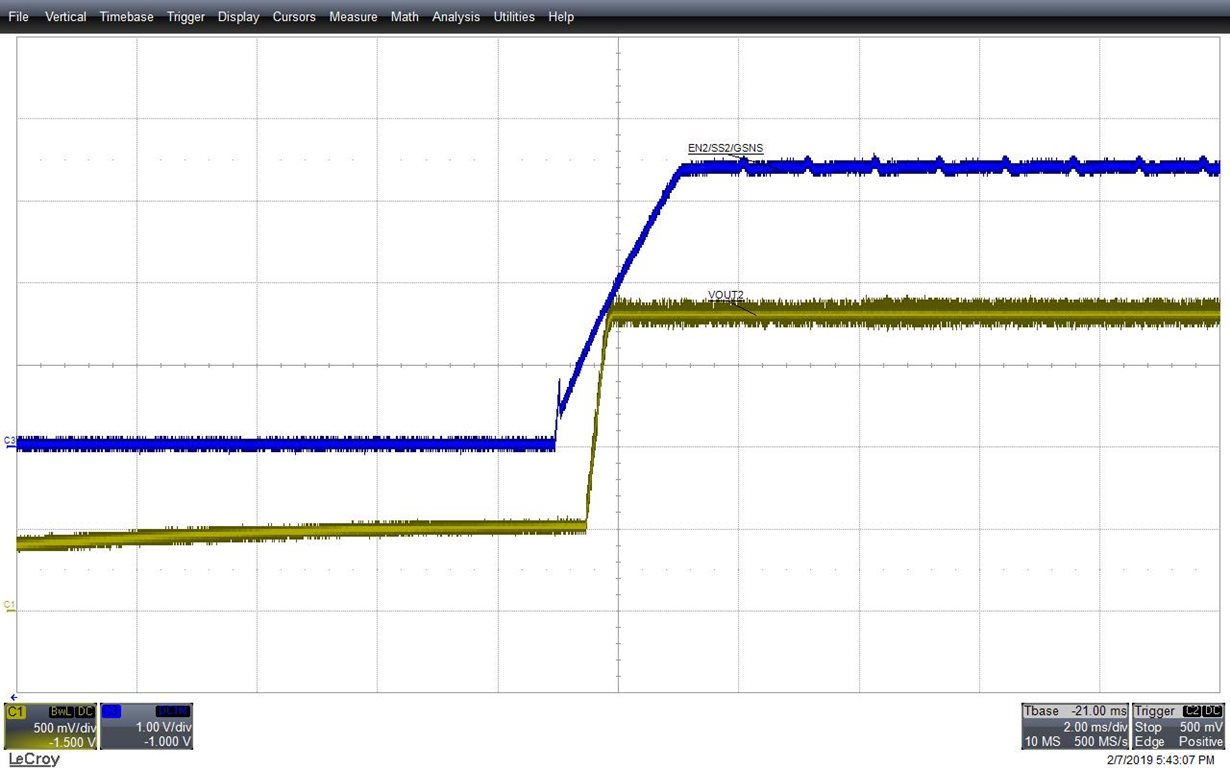
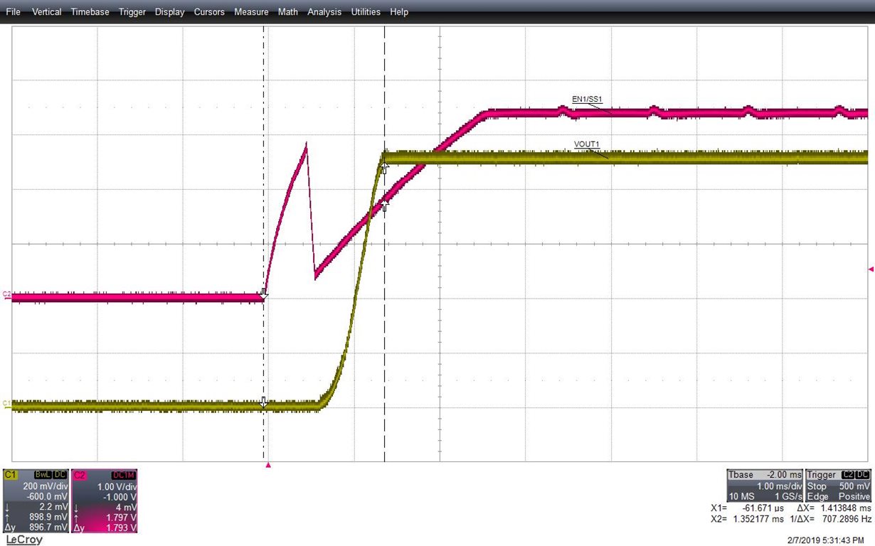
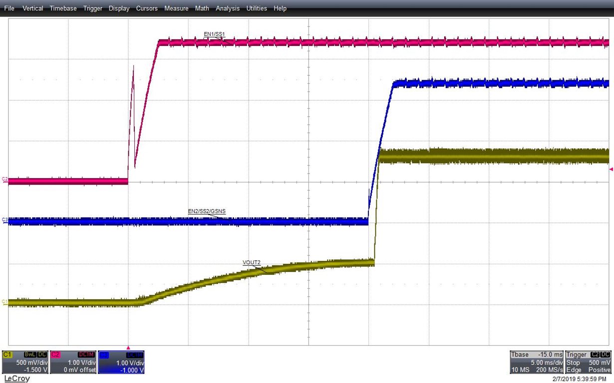
When I enable the CH1of the controller, VOUT1 (0.9 V) starts normally, but at the same time the VOUT2 voltage rise slowly about 0.5V and goes to 1.8 V when I enable the CH2.

My questions are:

Q1_ Is this behavior normal on CH2 or is something wrong in my design inducing this residual voltage? I would like no voltage on CH2 until I enable it (FPGA requirement).

Q2_ Why EN1/SS1 and EN2/SS2 don’t reach BP6 as observed in simulation ? (it seems to be clamped at half BP6)

Find attached my schematic and 3 waveform captures:

EN1&VOUT1

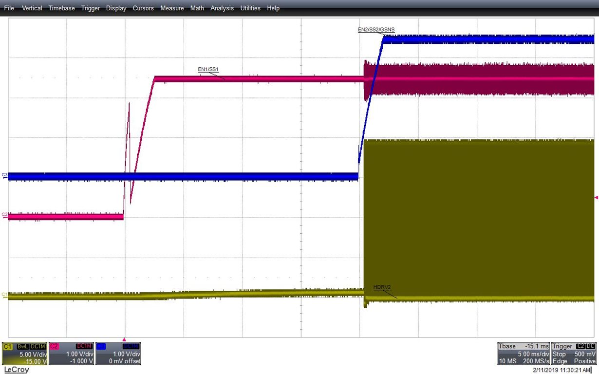
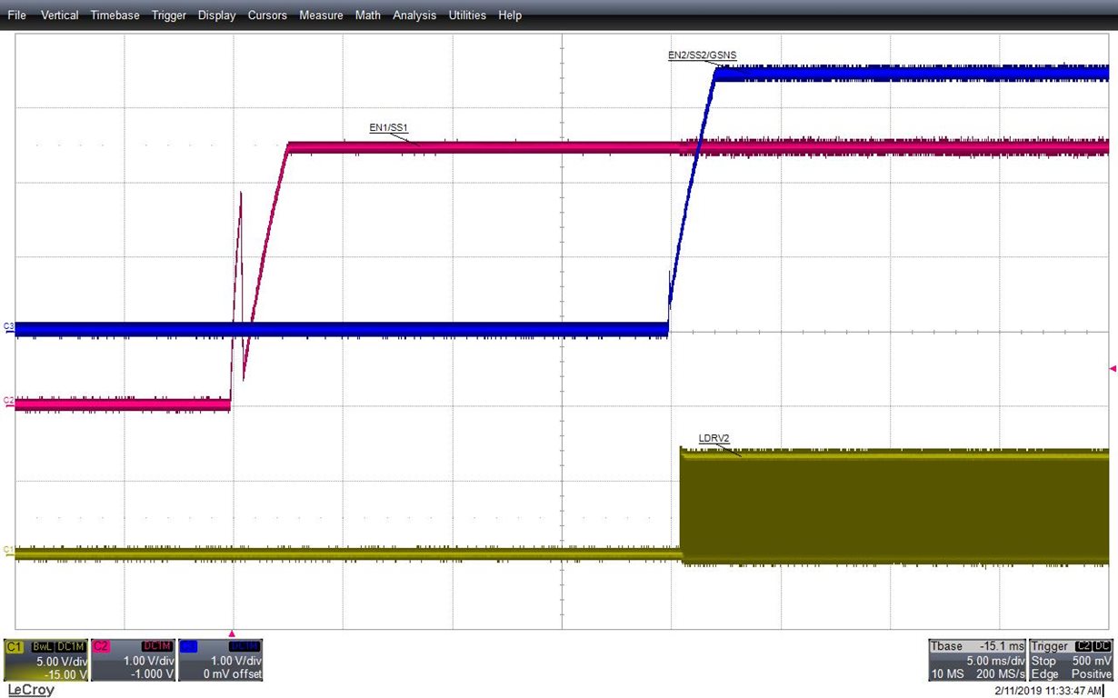
EN1&EN2&VOUT2

EN2&VOUT2

Regards,

PatrickTPS40322_Dual_Output.pdf
  • Hi Patrick,

    Q1_ Is this behavior normal on CH2 or is something wrong in my design inducing this residual voltage? I would like no voltage on CH2 until I enable it (FPGA requirement).

    This behavior is abnormal. Before EN2 rises up, can you check if HDRV2 and LDRV2 are switching when EN2 is 0V? If HDRV2 and LDRV2 are not switching, probably the output voltage is charged by external current.

    Q2_ Why EN1/SS1 and EN2/SS2 don’t reach BP6 as observed in simulation ? (it seems to be clamped at half BP6)

    How EN1 and EN2 are controlled?
    These two pins should be turn on/off by MOSFET or open-drain pin.

    Thanks
    Qian
  • Hello Qian,

    Thanks for quick answer,

    Enable are controlled by one ADG836. It is an analog switch (CMOS). Find attached the schematic of the enable.

    Patrick

  • Hi Qian,

    You are right, the HDRV2 and LDRV2 start when EN2 is activated (attached waveforms) it means the regulator operates correctly. As you said there is a current leakage in my design between the VOUT1 and the VOUT2 because we can see the current starts to charge the output2 when the VOUT1 is enabled.

    Currently we are looking for this issue in our design. You can close the request.

    Again thank you very much.

    Patrick