This thread has been locked.

If you have a related question, please click the "Ask a related question" button in the top right corner. The newly created question will be automatically linked to this question.

TPS61028: Output droops, switch node stops after high current event

Part Number: TPS61028
Other Parts Discussed in Thread: TPS61020, TPS61029

Hello,

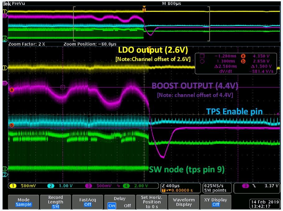
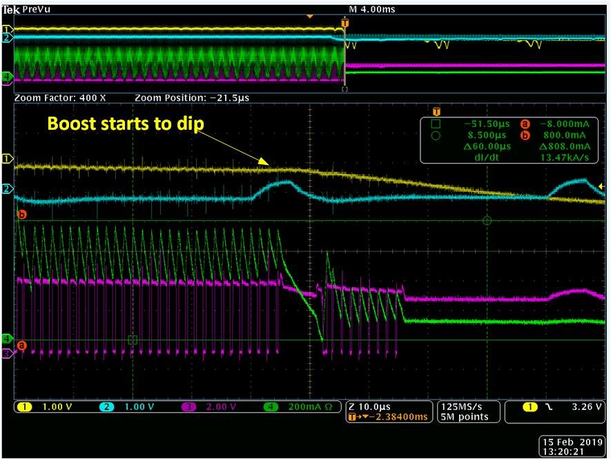
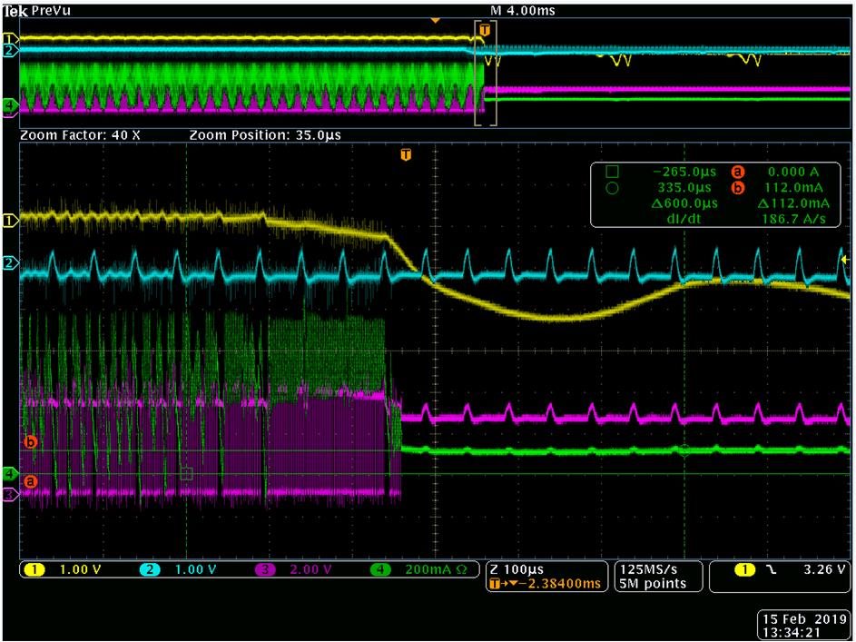
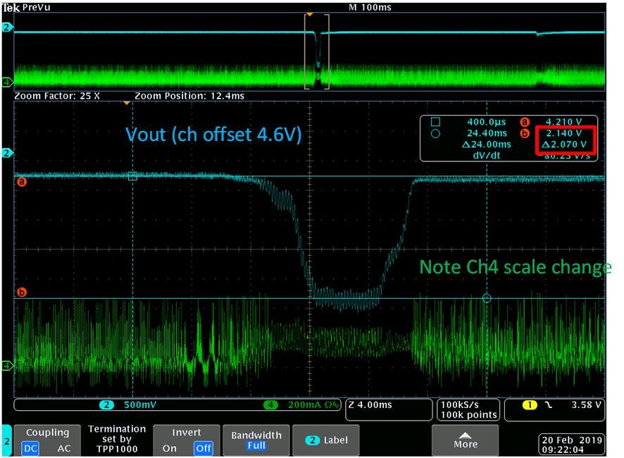
I am running into a reproducible issue on our design based on TPS61028.  As I load down the output by exercising all of the devices connected to it simultaneously (to simulate worst case conditions), I notice that the output drops significantly and the switching node also stops.  Initially I thought it might be due to reaching the current limit of 800mA output, but I do not read anything in the datasheet that would indicate that the switching would halt.

Attached is a waveform identifying the signals (note channel offset voltages do apply).  I cannot explain this phenomenon, unless the device is being 'tricked' into down conversion mode.  However, I would expect the device to recover and go back to switching properly.

Channel 2 (blue) is monitoring the enable pin of the device, to confirm that the controller does not get gliched to be 'disabled'

Channel 1 (Yellow) is monitoring the microprocessor's LDO output.

I have probed the SW node with a short ground probe during the higher current draws and low input voltage.  I did not see any switching node voltage in excess of 7V for a significant period of time.  Peak switching voltage was about 7.6V for approximately 5ns (low energy), measurement acquired with short ground probe and full bandwidth (1GHz).

Inductor choice is 4.7uH (Bourns SRP-2510A-4R7M).  10uF ceramic cap on input. 2.2uF and 22uF ceramic on output with 100m in series for ESR.  LBI is grounded.  LBO is not connected.  PS is tied to VIN.  FB resistors are 2Mohm and 270kOhm.

Layout of the design is very similar to that of the datasheet recommendation in section 13.

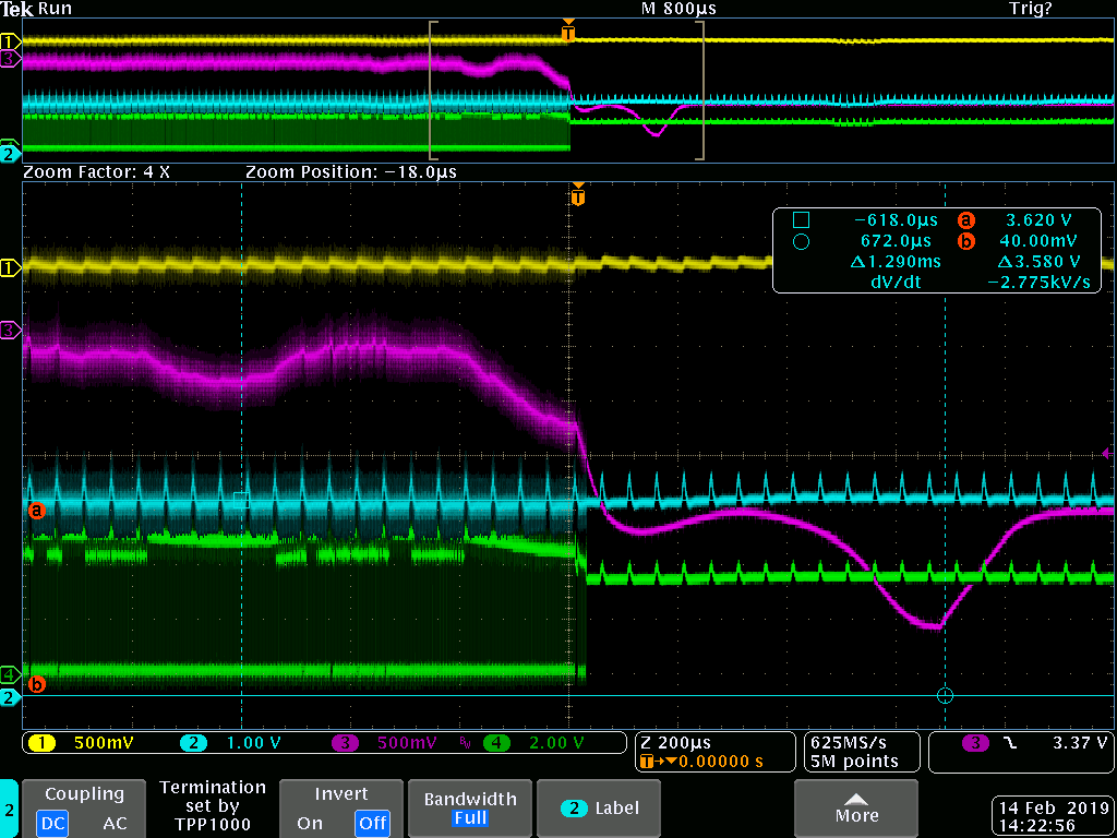
For thoroughness, I've also attached a waveform with the input voltage probed (approximately 3.6V).

  • Hi Daniel:
    It's glad to see the professional waveform and detail description. So clean and helpful.

    There is a unstable time before it stops switch. I thought it drops below VIN and catch the pre-charge function( as overload protection).
    Please see detail explain in the page 4 Return to Pre-Charge of the application note. www.ti.com/.../slva387.pdf

    What's the load condition? May you share a detail value? you could try to increase the load slowly if you just test the maximum load capability. Or larger capacitor may do help if the .
  • Hi Minqiu, 

    Thank you for your quick response.  In the waveform, it does look like the input voltage (blue, channel2) is equal to the boost output voltage (channel 3).  However, there's a channel offset so they are not equal.

    Looking at table 1 in the application note you linked above, I believe this would be considered phase 1.  If this was the state the controller was in, then I would expect channel 3 (boost out) to be approximately equal to channel 2 (input voltage).  Because of the offset.  They are not equal.  Boost in = 3.6V and boost out = 2.85V (first figure in my post, measured using the screen markers).  This may be due to the loading of the peripheral components though (if the output current is limited).  Table 1 does not indicate any non-switching states.

    Regarding the load condition, we have the boost output connected to a few components, display driver, audio amplifiers, op-amp, and a user interface IC.

    I think page 5 might be the 'smoking gun' where the application note states:

    "To exit start-up and enter normal operation, the output voltage must rise to complete each phase and then move to the next. If the output voltage does not increase, the converter can become stuck in start-up mode. This problem often occurs due to a load on the output during start-up; the limited current is not enough to increase the output voltage to the next level. None of these phases has a time limit or timeout circuit with which to trigger shutdown or exit."

    Because we are not enabling or disabling the peripherals connected to the boost, they would be presented as a load.  This note does make quite a bit of sense for the behavior I'm seeing.

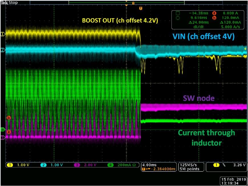
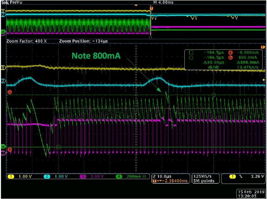
    I placed a current loop in series with the inductor and the behavior described in the application note can be seen (current dipping, voltage dipping and steady precharge current ongoing).

    Now, this begs the next question...  If the device is stuck in pre-charge mode, is there any potential long term damage to the device?  e.g. if the device was being run for multiple (10's of hours) in this condition, would it damage the controller?

    And as far as a solution, would you expect that this behavior would be changed if the controller IC was changed to TPS61020 (1500mA limit) or TPS61029 (1800mA limit)?

    Thank you for your help!

    Best regards,

    Daniel

  • Hi Daniel:
    Sorry that I'm out of office today. I have a cursory look at your supplement. Please wait me check after I back office.

    "In the waveform, it does look like the input voltage (blue, channel2) is equal to the boost output voltage (channel 3). However, there's a channel offset so they are not equal."
    Minqiu >> The Vout drops about 1V before it stops switch.

    And short speaking, I thought the issue could be simplified as:
    1. Why it stop switch?
    It's return to pre-charge since the Vout drops a lot. And the current limit is much smaller in this phase. So it couldn't reach the target to end the pre-charge.
    2. Why Vout drops?
    The peak current limit is 800mA(typcial.). You load may catch it. And if the load is heavier than the capability, the convert won't supply such VOUT as target.

    I thought it's better for you confirm your load condition. Have you calculated the value of Io needed?
  • Hi Minqiu,

    I agree with you regarding the switching stop. The Vout does drop, and since it drops a fair amount, the controller is likely going back to the pre-charge state.

    Regarding Vout drop, I will try to get the load output. In the layout, it is difficult to separate the load from the output of the switcher. I need to cut a few traces to allow this.

    Best regards,

    Daniel
  • Hi Daniel:
    The purpose that recommend you to confirm your load condition is to help you to do a better choice. It's more reliable and efficiency than testing one by one.
    Please let me know if there is other problem.
  • Hi Minqiu,

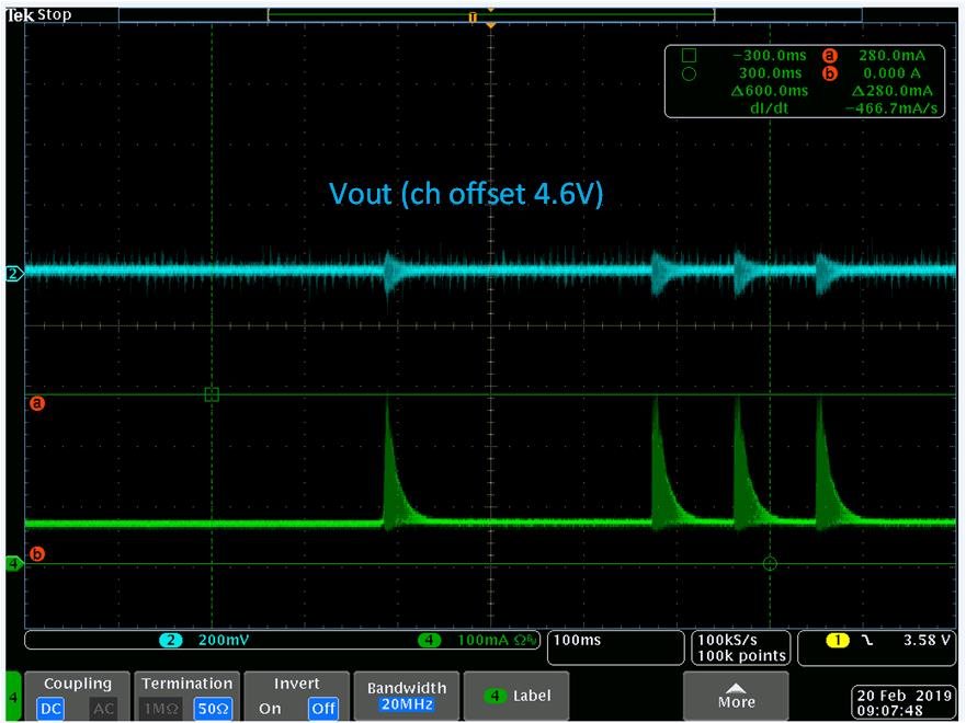
    I isolated the load and powered peripherals with a keysight power supply N6705B.  Current for both measurements was taken with a tek current probe attached to the load through a 22AWG wire.

    Steady state with all LED drivers exercised is about 68mA.

    I note that there is a high impulse current when the audio driver and speaker is exercised, topping out about 300mA (so about 230mA increase).

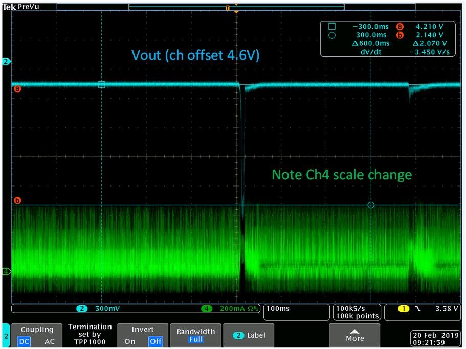
    I then re-connected the boost converter to the load, and performed the same exercise.  Note the 22AWG wire was connected between the switcher output and the load.  Bulk capacitance was on the switcher output side, then wire loop for current probe measurement, then load.

    I noted that the current was nearly double, noisy, and the output dropped significantly when exercising the audio amplifier in identical fashion.

    I am going to assume that the boost output (in the way the circuit has been designed in this implementation) cannot support this output, and the voltage drops until the load condition is removed.  Would this be a fair assumption in the behavior above?

    Additional question: Inductor selected is Bourns SRP-2510A-4R7M.  I noticed the DC Resistance of this inductor is about an order of magnitude higher than the recommended inductors in the datasheet.  Is Bourns SRP-2510A-4R7M an adequate choice for the application?  

    Thanks for your help!

    Daniel

  • Hi Daniel:
    Thanks for your details measurements. It seems reach the current limit and then the VOUT drops.
    It's recommended to replace the the TPS61028 with a larger current part. such as TPS61020, it's a pin 2 pin part, and easy for you debug. (You could apply some samples from TI.com to have a easy test)

    The resistance of the inductance will reduce the efficiency. Low efficiency will lead to larger Iin with same load in some way.
    It depends your system including cost, size, and other considering.