This thread has been locked.

If you have a related question, please click the "Ask a related question" button in the top right corner. The newly created question will be automatically linked to this question.

CSD18540Q5B: Using CSD18540Q5B in Saturation mode as a current sink (constant 4.5A). Will there be any issues?

Part Number: CSD18540Q5B

Hi,

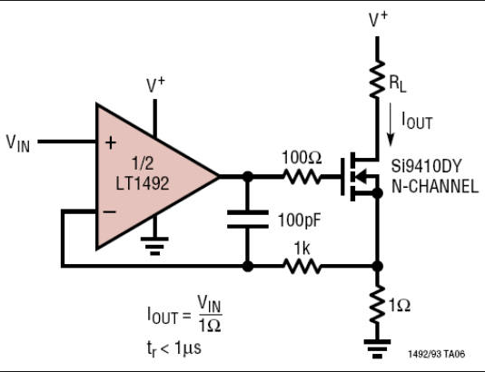
I've designed a circuit using the CSD18540Q5B as a constant current sink for a short time duration (4.5 Amps for 20mS) and successfully simulated in spice. The CSD18540Q5B is operated in the Saturation region and is controlled by a Op Amp (similar to the attached picture but with a much smaller sense resistor). I verified the MOSFET would not be damaged based on the power dissipation using calculations for junction temperature and derated SOA plot in datasheet based on case/ambient temperature. However, I was warned in a peer design review that some MOSFETS don't "like" to operate in the Saturation region and that planer gate MOSFETS works better in the saturation region but Trent or Super junction structures have areas of gate that can saturate and cause the MOSFET to blow up. Do I need to worry about the CSD18540Q5B having an issue with operating in the Saturation region as described above and blowing up based on the architecture of it's design?

Thanks, Nick

  • Hi Nick,
    Thank you for your questions. Can you give me more details on the application? What is VDS during the 20ms when the FET is sinking 4.5A? I'm looking into this further to determine if there may be potential problems.
  • Hi John,

    There is a 2 ohm and 1 ohm resistor in series and these are between the supply and the CSD18540Q5B. The supply can range between 15V and 34V. When the supply is at 15V VDS = .543V (at 55°C) to 3V (at -55°C) and at 34V supply VDS = 19.55V (at 55°C) to 22.08V (at -55°C).

    As mentioned, the circuit is only turned on for 20 milliseconds and draws 4.5A continuously (nominally). Note: the simulation also gave the following results:

    For 15V-34V design ran sim from -55°C to 125°C in 5°C steps at 15V and 55V supply:
    • Current: 3.837A (15V supply, -55°C) to 4.721A (34V supply, 55°C).
    • 2 Ohm R power: 29.45W (15V, -55°C) to 44.58W (34V supply, 55°C)
    • CSD18540Q5B power for 20mS: 2.57W (15V supply, 55°C) to 92.54W (34V supply, 125°C)
    CSD18540Q5B Junction Temp: 72.44°C (15V supply, 55°C) to 122.82°C (34V supply, 125°C)

    Thanks,

    Nick
  • Hi Nick,
    It looks like you have done your homework analyzing and simulating the circuit. I have consulted with a colleague. We've heard similar comments about trench vs. planar but not SJ vs. planar. In any case, planar devices are typically larger die size for the same rds(on) when compared to trench or SJ devices. As such, they tend to have better SOA and thermal handling capabilities. However, we don't believe you will have any issue as long as the device is operating within the SOA boundaries with the appropriate thermal derating. Please note, the SOA curve in the datasheet is based on testing at 25degC and derating is recommended for higher operating temperature. I may have already pointed you this blog: e2e.ti.com/.../understanding-mosfet-data-sheets-part-2-safe-operating-area-soa-graph, and video training: training.ti.com/understanding-mosfet-datasheets-safe-operating-area-soa, which are very useful for this type of application.

    Some vendors play fast and loose with SOA being typical performance. However, TI believes ours as the worse case capability we would guarantee (even if we don’t guarantee it the same we would an abs max table which is tested in production). All of our testing is done to failure and we further derate the SOA curves from that data insuring adequate design margin. This 60V device technology family has been tested against other vendors silicon and we confidently stand by its robustness.
  • Thanks John,

    Your a big help!

    Nick