This thread has been locked.

If you have a related question, please click the "Ask a related question" button in the top right corner. The newly created question will be automatically linked to this question.

UCC24610: Drain-Source Voltage Clamp Architecture for UCC24610

Part Number: UCC24610

Hi there,

I am attempting to figure out the voltage clamp architecture on the TI UCC24610 chip for the drain and source sense pins:

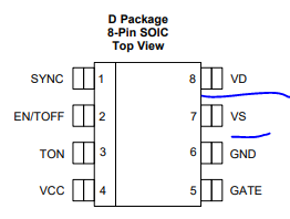
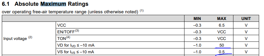
The datasheet notes that it has a ~50V maximum rating:

Would any of the applications or design engineers in the BU happen to know the internal clamp architecture? Is it a internal zener, rail to rail clamp with a zener rail clamp, etc? Thank you!

Best,

Oscar

  • Hello Oscar,

    The UCC24610 does not have an internal clamp. It is up to the designer to make sure these pins do not exceed the absolute maximum rating. This can be controlled by the transformer turns ratio and the maximum output voltage. I would add 25% margin just to be safe.

    Vds(max) ≈( Vinmax*Ns/Np + Vout*max)*1.25

    Regards,

    Mike