This thread has been locked.

If you have a related question, please click the "Ask a related question" button in the top right corner. The newly created question will be automatically linked to this question.

LMG5200EVM-02: Failed high-side switch

Part Number: LMG5200EVM-02
Other Parts Discussed in Thread: LMG5200

Hello,

While testing the board at switching frequencies (1 Mhz and 10 MHz) with variable load resistor of 0 to 36.3 ohms, the high side GaN Mosfet failed. I measured the input impedance and it was very low (6 ohm). What might be the reason for this? The datasheet of LMG5200 says that it is possible to switch the transistors up to 10 MHz, so I don't think it is high switching frequency that caused this. 

Note: I have replaced the on-board inductor with a planar spiral inductor (single layer) of 280 nH. In the later stages, I have to test with double layer coils with different winding layouts. 

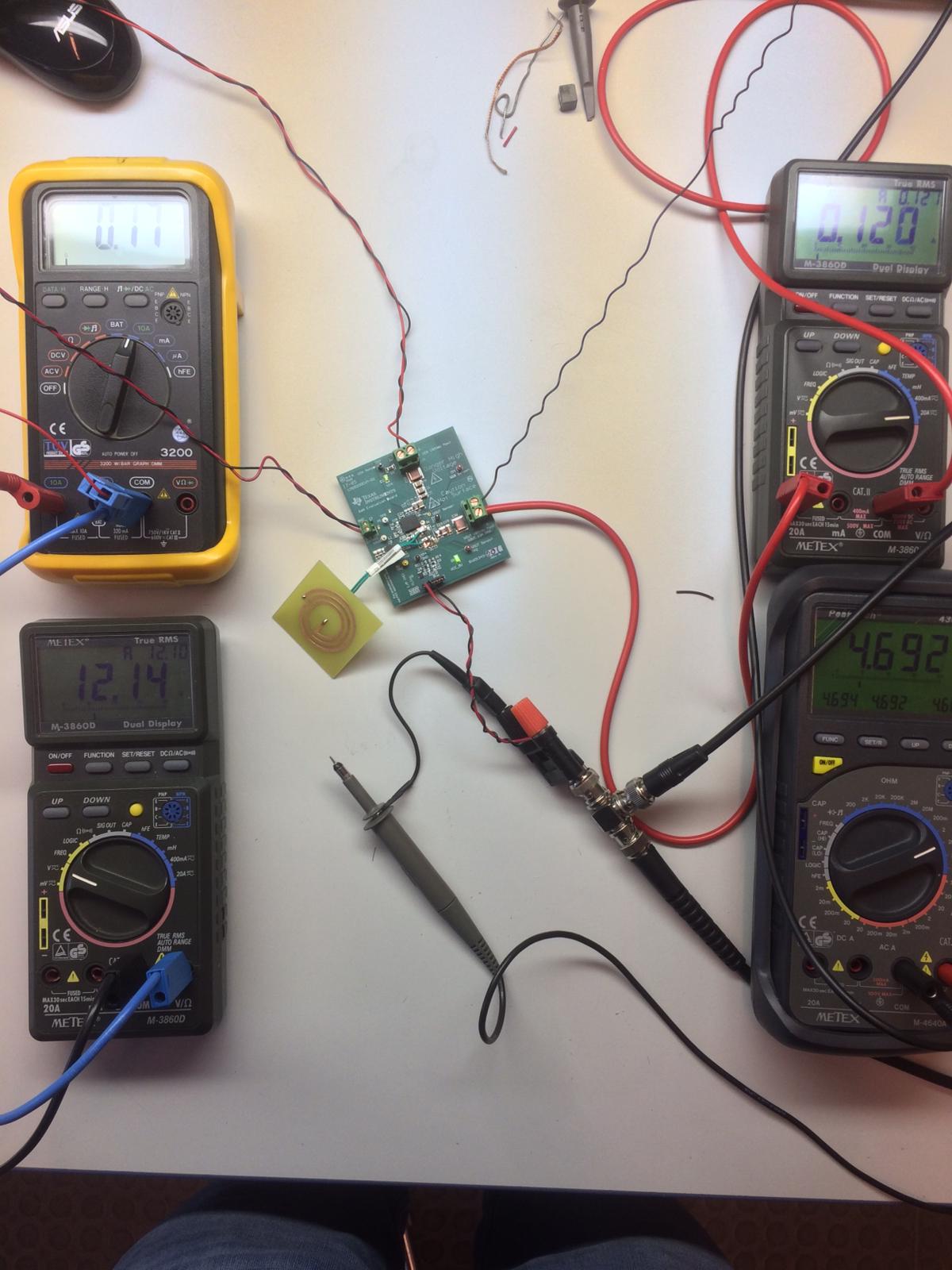
One more question, when I see the output at switching node I cannot see any deadtime generated like shown in the user guide of the evaluation board. So I placed output of the PWM signal from signal generator and Switch node output and tried to measure it. Is it the right way to do so? 

Thank you,

Girish

  • Hello Girish,

    To answer your question,

    1. For the failure, the most possible reason might be overheating. Have you watched on the temperature of the devices? Also was the VDD power stable? 10MHz is not a problem for the device. Also did you have enough dead time?

    2. For the waveform that you see, first of all you had bandwidth limitation turned on, which prevents you from seeing accurate waveform. Is the blue one switching node? You can make your dead time large enough and pull enough current from the inductor. This way you will see the dead time negative switching node voltage as the inductor will flow through the third quadrant of the device.

    Thanks and regards,
    Lixing
  • Hello,

    1. I did not measure the temperature of the device, but as far as I can tell it was not hot. Yes, the VDD (power supply) was stable 12 V and the bias voltage was set to around 7 V.

    2. Yes, the blue one is the switching node signal. How to make dead time large? Do I need to change R14 and R2 to achieve this? It is says in the user guide that inherent dead time need not changed and board can be evaluated without doing so.

    I have ordered a replacement chip. Do you have any tutorials on how to solder this?

    Could you also please tell me how to do dead-time measurement?
  • Hello Girish,

    Sorry for the late reply due to my travelling.

    1. If it is not very hot, maybe it is not the loss that causes the failure. However, there might be some risk that you do not have enough dead time to damage the half bridge through shoot through. What is the dead time that you have added?

    2. During dead time, there would be a negative current across the switching node due to the third quadrant conduction of the low side FETs. By this way you can tell what your dead time is. However, please make sure that you turn on the full bandwidth of your scope since this transition is hard to observe. There is no dead time generation inside LMG5200. Therefore, you have to make the dead time when you are inputing the PWM signals from your controller.

    3. Regarding the soldering of the FET, I suggest you use solder paste and then allow some heat to melt the solder paste. This could give you the best result.

    Thanks and regards,
    Lixing