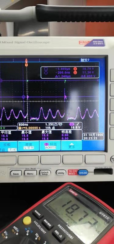
Dears:
Could you kindly help to check the schematic?
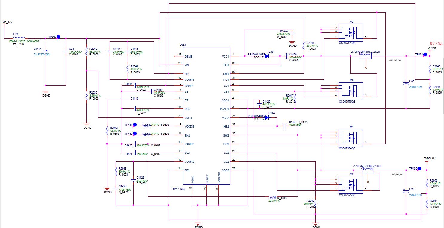
Since there is no output of 5V, and there is no signal testing Nmos' G pot and S pot.
There is no voltage testing FB PIN.
How is the state of PIN31 and PIN32?
Pls. give some advice.
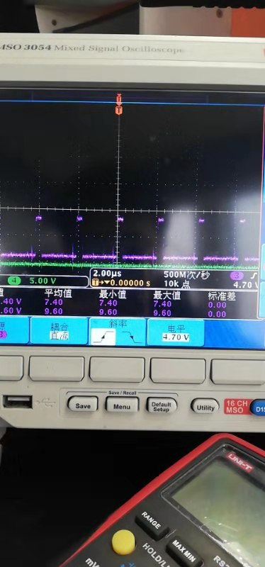
Dears:
Could you kindly help to check the schematic?
Since there is no output of 5V, and there is no signal testing Nmos' G pot and S pot.
There is no voltage testing FB PIN.
How is the state of PIN31 and PIN32?
Pls. give some advice.