This thread has been locked.

If you have a related question, please click the "Ask a related question" button in the top right corner. The newly created question will be automatically linked to this question.

TPS65262: TPS65262 - loop compensation

Part Number: TPS65262
Other Parts Discussed in Thread: TPS65265

Hello Team,

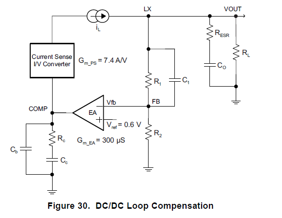
On the TPS65262 Datasheet on page 26, there is a calculation which involves a “RL” which is not described any further.

On the Schematic it looks like “RL” means a resistive load. I am a little confused because of the Arrow which points away from VOUT which suggests that there is another Load or something else.

This would make a calculation with RL useless.

Also, if “RL” means the complete load, I wonder why they don’t calculate with the average Output current instead like everywhere else in the datasheet.

  • Can you comment farther RL?

 In addition to that: Is there an easy way to calculate the FeedForward Capacitor C1?

thanks,

SunSet

  • Hi, SunSet 

    Comments: 

    1. RL is load resistance, it is equal to Vout/Iout, so it is used for calculating pole at Vout in equation 17. 

    Under different loading(Iout), the RL is different, and it is the DC value, so don't need to average it. 

    2. The Arrow stands for inductor current, because it has ripple, so it is needed to be averaged, in peak current model, it is modeled to ideal current source. 

    3. For usual application, suggest to set C1=22pF. 

    Besides, as a best practice, you can refer the EVM schematic for your design. TPS65262EVM schematic.pdf

  • Hello Ma,

    thanks for the info.

    Regarding the arrow, I meant the one next to Vout label. It looks that beside RL there is something else connected so RL is not the total load.

    Nevertheless from what you said RL is the total load out of Vout/Iout.

    For C1 do we have any formula to use to get also a direction and understand trade off between bigger values vs lower ones?

    I would assume that it may also be related to the R1 choice.

    Which cut off frequency should have combined with the feedback resistor?

    Thanks,

    SunSet

  • Hi, SunSet 

    1. Oh, got you, the arrow at Vout does cause some misunderstanding. The RL is the total load. 

    2. C1 is feedforward capacitor, C1 and R1 will form a Zero which can enlarge bandwidth and boost phase margin. 

    Usually, we set Zero at slightly higher loop bandwidth. 

    TPS65265 is also a peak current mode buck, you can refer the compensation description in page 29 of datasheet. 


    3. What is the cut off frequency? 3dB bandwidth frequency? it is not related with feedback resistor. 


  • Hello Ma,

    thanks for your inputs. For point 3 I meant what you have pointed out on point 2. I was expecting a relationship between C1 and R1.

    ...not a cut off (Pole) ....but a Zero instead.

    Thanks,

    SunSet

  • Hi, Sunset 

    The Zero is equal to 1/(2*pi*C1*R1).