This thread has been locked.

If you have a related question, please click the "Ask a related question" button in the top right corner. The newly created question will be automatically linked to this question.

TPS40210: difference vs webdesign

Part Number: TPS40210
Other Parts Discussed in Thread: CSD18543Q3A, CSD18542KTT

Hi,

I use the design below from the webdesign (I don't know if the link works)

webench.ti.com/.../SDP.cgi

Some few values are very slightly different (for normalized one)

I encounter a problem to sourcing enough current from this design. The current parameters was selected for 1.5A and I can barely source more than 100-200mA before seeing voltage decrease (with a voltmeter and a LED is used to check that 48V is present, it starts blinking when regulation start to do not works).

I use resistive load for testing, with 100 ohms the problem is clearly visible.

I thought as my power supply was not close to the chip that it was the mainly reason, but adding 47µF close to the initial Cin didn't improve the results.

All components are all grouped on a small area.

Thanks for your help.

  • Hi Cedric,

    The Webench link works. Thank you for designing with the TPS40210. I understood that your final board is based on the Webench design. Could you share your final schematic that you used to design your own PCB? Please make sure the part values or part numbers are accurately labelled.


    Thanks,
    Youhao Xi, Applications Engineering.
  • Hi Youhao,

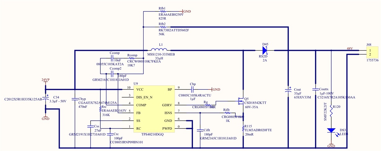
    please find attached the picture of the schematic for this function.

    thank you.

  • I think there is a missing junction between D45 cathode + and Cout, I check this and report if solved.
  • no missing junction, problem come from other thing.
  • Part Manufacturer Part Number Mounted Quantity Footprint (mm²) Description
    Cbyp Taiyo Yuden GMK212BJ474KG-T CGA4J3X7S2A474M125AE 1 6.75 Cap: 470 nF Total Derated Cap: 470 nF VDC: 35 V ESR: 1 mΩ Package: 0805
    Ccomp2 Samsung Electro-Mechanics CL21C181JBANNNC GRM2165C1H181JA01D 1 6.75 Cap: 180 pF Total Derated Cap: 180 pF VDC: 50 V ESR: 0 Ω Package: 0805
    Ciflt Samsung Electro-Mechanics CL21C181JBANNNC GRM2165C1H181JA01D 1 6.75 Cap: 180 pF Total Derated Cap: 180 pF VDC: 50 V ESR: 0 Ω Package: 0805
    Cout Panasonic 63SXV33M 63SXV33M 1 106.09 Cap: 33 µF Total Derated Cap: 33 µF VDC: 63 V ESR: 25 mΩ Package: 8x11.9
    Css MuRata GRM155R71A273KA01D GRM2191X1H273JA01D 1 3 Cap: 27 nF Total Derated Cap: 27 nF VDC: 10 V ESR: 1 mΩ Package: 0402
    L1 Coilcraft MSS1210-333MEB MSS1210-333MEB 1 204.49 L: 33 µH DCR: 33 mΩ IDC: 5.9 A
    Rcomp Yageo RC0201FR-0718K7L CRCW080518K7FKEA 1 2.08 Resistance: 18.7 kΩ Tolerance: 1.0% Power: 50 mW
    Riflt Panasonic ERJ-6ENF1001V CRG0805F1K0 1 6.75 Resistance: 1 kΩ Tolerance: 1.0% Power: 125 mW
    Rsense Stackpole Electronics Inc CSR1206FK20L0 TLM3ADR020FTE 1 10.92 Resistance: 20 mΩ Tolerance: 1.0% Power: 500 mW
    Cbp Kemet C0805C105K4RACTU C0805C105K4RACTU 1 6.75 Cap: 1 µF Total Derated Cap: 1 µF VDC: 16 V ESR: 15 mΩ Package: 0805
    Ccomp TDK CGA4C2C0G1H103J060AA 08055C103KAT2A 1 6.75 Cap: 10 nF Total Derated Cap: 10 nF VDC: 50 V ESR: 0 Ω Package: 0805
    Cin TDK C2012X5R1H335K125AB C2012X5R1H335K125AB 2 6.75 Cap: 3.3 µF Total Derated Cap: 3.3 µF VDC: 50 V ESR: 2.8 mΩ Package: 0805
    Crc Samsung Electro-Mechanics CL21C910JBANNNC CC0805JRNP09BN101 1 6.75 Cap: 91 pF Total Derated Cap: 91 pF VDC: 50 V ESR: 0 Ω Package: 0805
    D1 SMC Diode Solutions SK220ATR RS2D R5 1 37.34 Type: Schottky VRRM: 200 V Io: 2 A
    M1 Texas Instruments CSD18543Q3A CSD18542KTT 1 18.49 VdsMax: 60 V IdsMax: 35 Amps
    Rg Vishay-Dale CRCW040219R1FKED CRG0805F10R 1 3 Resistance: 19.1 Ω Tolerance: 1.0% Power: 63 mW
    Rrc Panasonic ERJ-6ENF3163V ERA6AEB3163V 1 6.75 Resistance: 316 kΩ Tolerance: 1.0% Power: 125 mW
    U1 Texas Instruments TPS40210DGQR TPS40210DGQ 1 23.6
    Rfb1 Vishay-Dale CRCW0402825RFKED ERA6AEB8250V 1 3 Resistance: 825 Ω Tolerance: 1.0% Power: 63 mW
    Rfb2 Susumu Co Ltd RR1220P-563-D RK73H2ATTD5602F 1 6.75 Resistance: 56 kΩ Tolerance: 0.5% Power: 100 mW
    Coutx TDK C3216X7R2A105K160AA C3216X7R2A105K160AA 1 10.92 Cap: 1 µF Total Derated Cap: 1 µF VDC: 100 V ESR: 4.58 mΩ Package: 1206_180

    In yellow, the parts that are mounted on my design and different from the left (mainly for size 0805 instead of 0603 or 0402 or normalized values)

  •  here is a curve with 470 ohms load (100mA)

  • Hi Cedric,

    Youhao is out of the office and will be back next Tuesday. He will be able to support your questions then.

    Thanks,

    Garrett
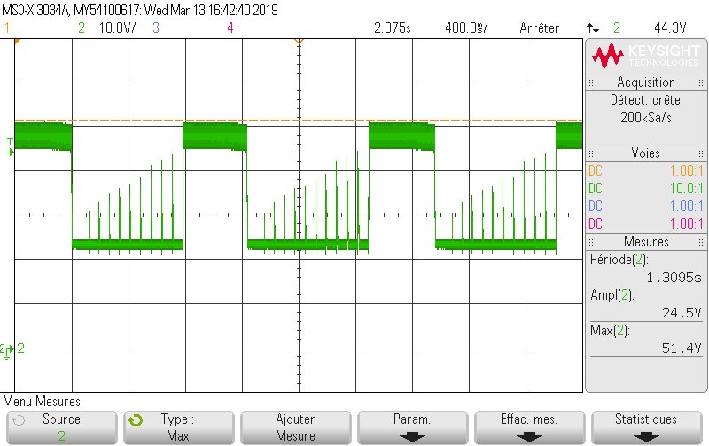
  • With a different mosfet (Rdson and Cgate too), I suspect the SW Ipk to be above the Isense triger value and cut (the green curve is at 24V when Mosfet is off long enough and we can see some starting sequence before new switch off and it continously repeat)

    because in the chart of the initial simulation we can see that SW Ipk is max 3.5A.

    What is the equation to calculate this SW Ipk ?

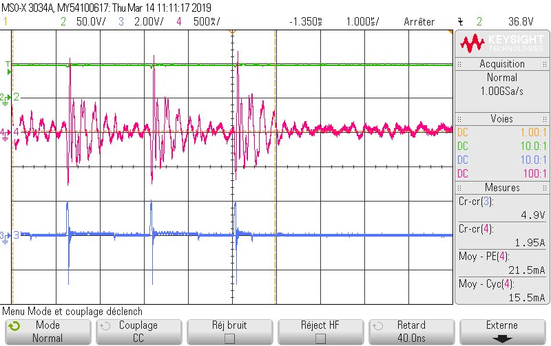
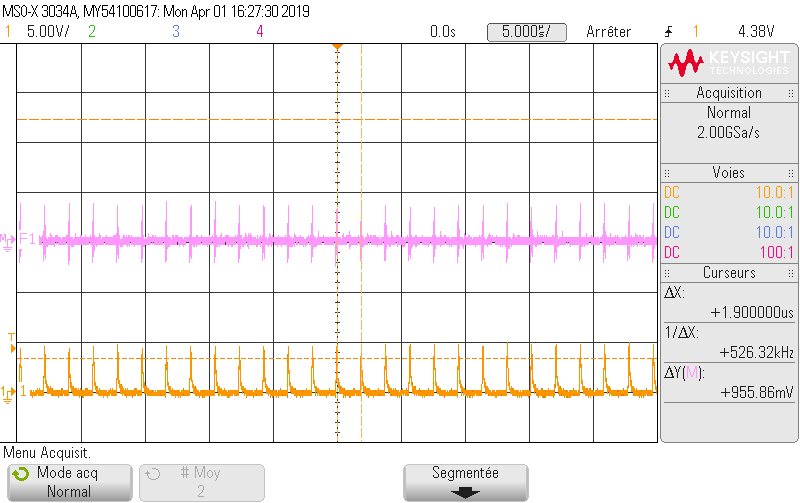
    on the curve below we can see in blue the voltage across Rsense (before low pass filter to ISNS pin of the TPS40210)

    the pink one is the current flowing through the 470R load on my 48V output with a clamp amperemeter.

  • Any idea regarding this issue ?

  • HI Cedric,

    Equation 16 of the datasheet can be used to calculate the switch peak current. The terms in the denominator is the peak current formula.

    In your post of March 13th, what is exact that green curve? The Vout?

    In your post of March 19th, trace 3 (blue) is approach 2V. It cannot be the current sense signal because it is well beyond the peak current limit (150mV Typical), and the circuit will trigger the Hiccup mode. Also, your resistance is only 20 mOhm, 2V implies 100A. Would you please confirm?

    Thanks,
    Youhao
  • Green curves of March 13 is the 48V output (you have the max value ant the amplitude when it falls to 24V, M1 OFF)
    The blue is the sense voltage (but I don't remember if it's at the Risns pin or behind the low pass filter on the ISNS pin directly). The pink one is the current across the 470 resistive load on output, measurement taken with a clamp current probe.

  • According to equation 16 I found a 0.107 ohms for Rsense if Iout=500mA and 0.043 ohms for Iout=1.5A.

    Does it means that my Rsense is too low then it made trip the TPS40210 ?

  • Higher resistance makes more easier to trip the current limit, but not the other way around. You waveform shows much higher current than 0.5A if your sense resistor is 0.107. Can you double check your sense resistor value, and make sure it is really 20 mOhm? Your waveform shows almost 2V on the current sense trace.
  • I'm sure, marking is R020 on the resistor.

  • So, please remeasure the voltage waveform of the sense resistor. Your previous scope picture shows 2V, and it does not make sense. Just need to verify if it is really the case. If it is still 2V, please check your soldering and connections.

    Thanks,
    Youhao
  • Hi Cedric,

    Any update? Can I assume the issue is resolved? We are required to close the thread if no activity for a few days. You can always reopen it by a new post.

    Thanks,
    Youhao
  • Hi Youhao,

    no, the problem is not solved, I had to work on another project for few days.

    The sense resistor is correct, the measure is taken directly on the sense resistor

    there is always a current flowing through the 0.02R resistor, even without load resistor on 48V output, below are the pictures.

    Is it normal ?

  • see last post with pics attached.
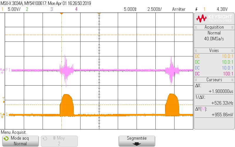
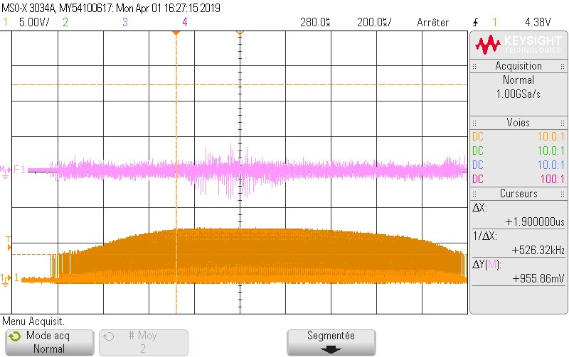
  • below more pics with in addition to Vsense (pink) the VGS of the MOSFET in orange (always without load).

    closer view.

    closer view

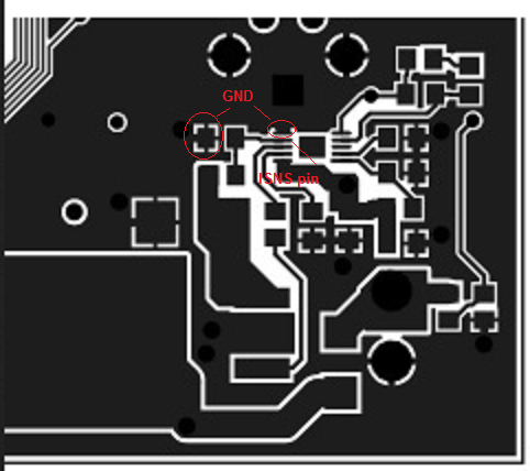
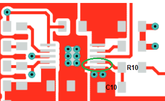
  • I see a lot of noise on your current sense pin. You Ciflt ground pin is on the wrong location. Please place Ciflt directly across the ISNS and GND pin. Currently your Ciflt sits on the same polygon as the current sense resistor. Please also refer to our EVM layout example. Your Ciflt ground pad is far away from the IC GND pin.
  • Hi,

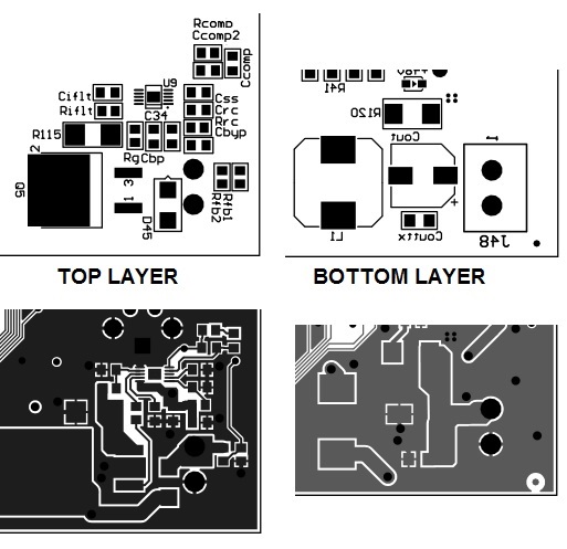
    see pics attached there is less than 1cm between Ciflt and TPS40210, it's difficult to be closer.

    Do you think layout is the only reason because circuit doesn't works ? (even from 0.1A) ?

  • Hi the curves are recorded at Rsense (not ISNS pin which is through the low-band filter)
  • below the part that looks similar of the EVM.

    the chip capacitor is just flipped of 180° but the position is similar and the GND (not visible on the picture) is wired in the same way to the sense resistor.

  • Hi,

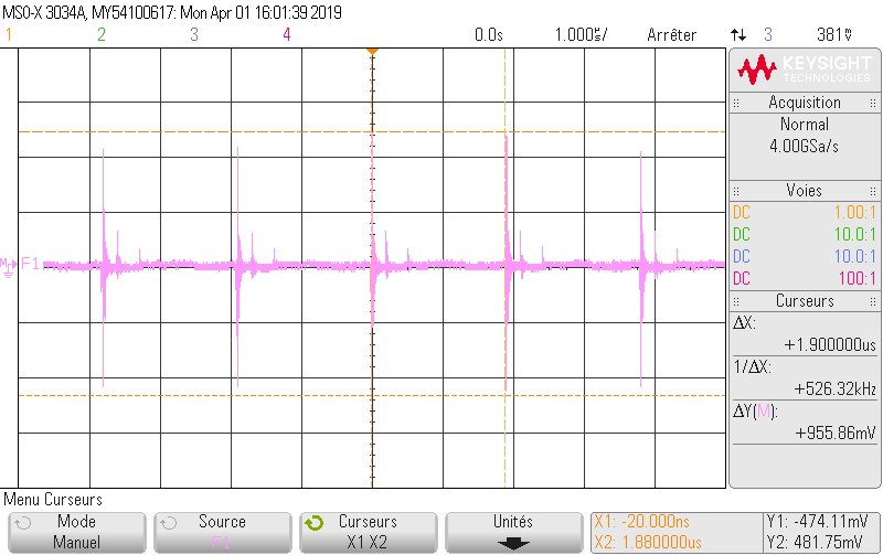
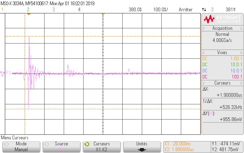
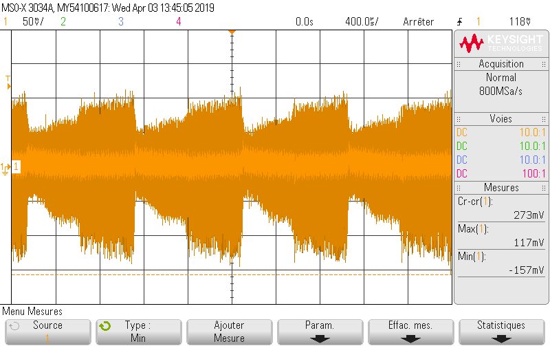
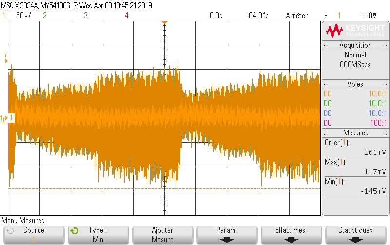
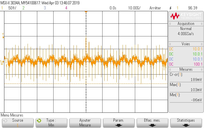
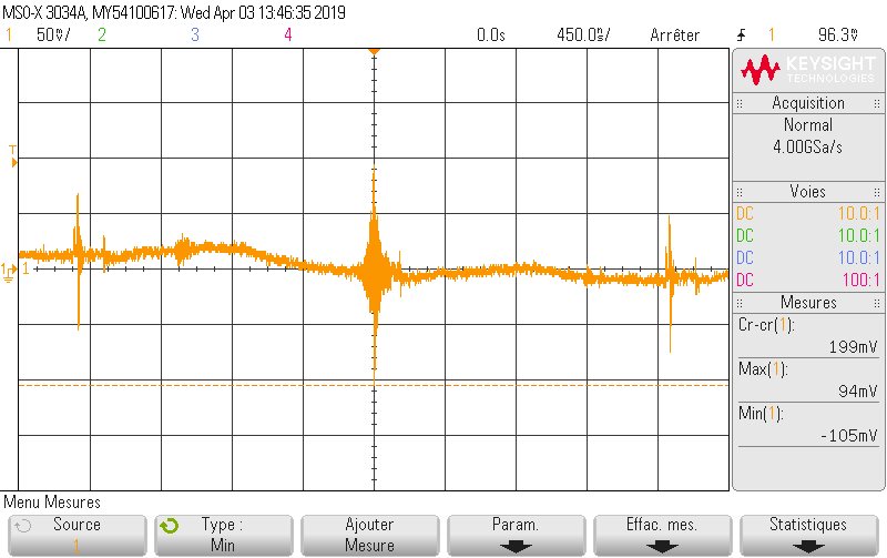
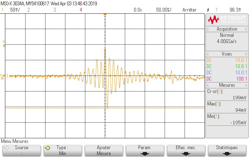
    below are some screens recorded directly to the ISNS pin.

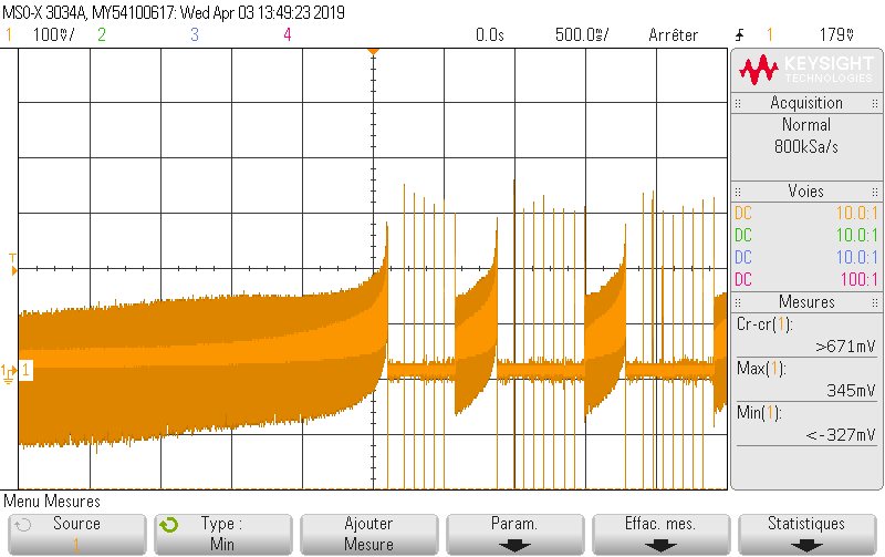
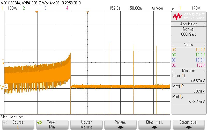
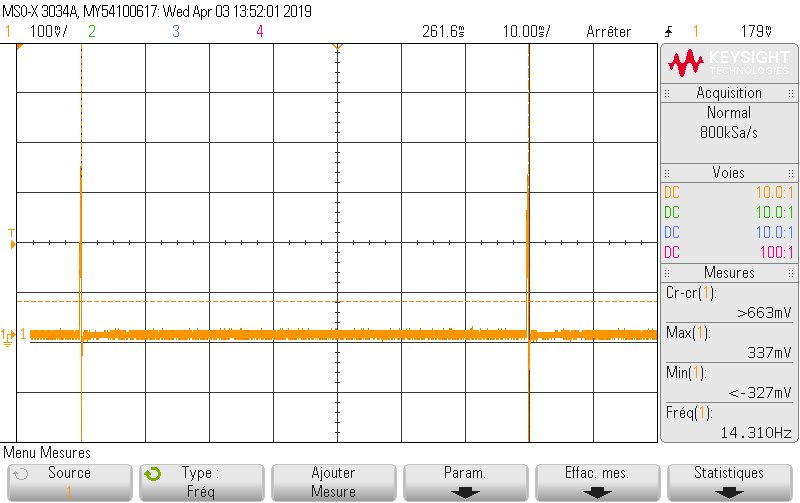
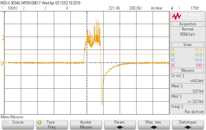
    annexe 1: no load ISNS voltage

    annexe 2: no load ISNS voltage close-up view

    annexe 3: no load ISNS voltage closer again

    annexe 4: no load ISNS voltage closer again

    annexe 5: no load ISNS voltage closer

    annexe6: 470R load ISNS voltage (beginning of output cut off)

    annexe 7: 470R load ISNS voltage (closer view)

    annexe 8: 470R load ISNS voltage (closer view)

    annexe 8: 470R load ISNS voltage (closer view)

    it's visible than 150mV are reached to the ISNS pin, but how limiting this ?

  • Hi,
    The responsible engineer is out now. We will reply by 4/12.
    Regards,
    EL
  • Hi, ok

    why is there any additionnal resistor (R3) on the SS pin on the EVM ?

    I see no explanation in the datasheet about that.

    Regards.

  • Hi
    The responsible engineer is out now. You will be able to get a reply soon.
    Regards,
    EL
  • Hi, any help from the engineer would be appreciated.

    it's the last unworking function on our PCB.

    Best regards.

  • Hi
    The responsible engineer is still out of office now. He will reply by 4/23.
    The major purpose of R3 resistor is to minimize the start-up delay from 'SS start rising' to 'start switching'
    Regards
    EL
  • Hi, I made some improvments by changing the schottky diode.

    the previous one had a 1.5V forward drop, I changed for a 0.85V forward drop.

    can it explain the instability as the feedback voltage is taken behing the schottky diode ?

    I could sink near to 250mA for the moment, I have to perform other test and check if I can sink more while still being stable and not trig the overcurrent protection..

  • Hi, problem seems resolved, but I wish have a feedback for my last question from app engineer if possible.

    Regards.