This thread has been locked.

If you have a related question, please click the "Ask a related question" button in the top right corner. The newly created question will be automatically linked to this question.

UCC27211A-Q1: Reducing ripples

Part Number: UCC27211A-Q1
Other Parts Discussed in Thread: CSD18537NKCS, , UCC27282

Hi, 

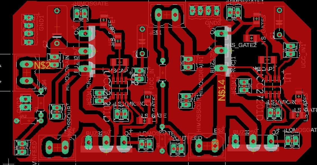
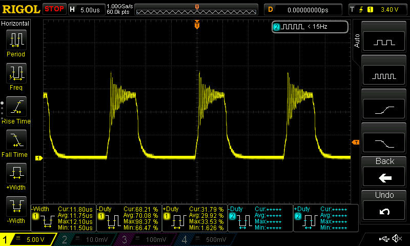
I'm using UCC27211A-Q1 to drive two N-channel MOSFETs (CSD18537NKCS) synchronously. I want to reduce the ripples for the switching waveform. Please find the attached screenshots of the switching waveforms and the PCB layout of the circuit. Do the ripples have to do anything with the dead-time between the two complementary PWMs supplied by controller to HI and LI pins of the UCC? How can I reduce the ripples for the switching waveform?

  • Hi Tejas,

    Sorry you are having difficulty with our device.

    Are you sure this is real? It might be a measurement issue.

    Please read this blog for more information: e2e.ti.com/.../how-you-measure-your-ripple-can-make-you-or-break-you

    If you verify it’s not a measurement issue, let us know any we can check other things with you.
  • Hi,
    The ripple is initially less and it's increasing as I'm increasing the input voltage. So I believe that it is not a measurement issue.
    Is there any problem with the PCB layout? The value of the bootstrapping capacitor is 1uF. Does the dead-time between two complementary PWMs have an effect on the observed ripple?
  • Hello Tejas,

    I work with Don supporting this device and will work to address your concerns.

    I have a couple of comments about the layout. The ground connection from the VDD capacitor to the driver  VSS pin is very long trace length. This connection needs to be a short/low inductance trace to minimize ringing from trace inductance. Can you connect pin 7 of the driver IC to the ground plane close by, on the right side of the IC. Also, the connection from VSS of the IC to the low side MOSFET source is a narrow trace. Can the two pin component connecting to pin 6 move to the left to allow a wider trace from pin 7 to the MOSFET source?

    The bootstrap capacitor value of 1uF seems larger than is necessary, assuming the minimum switching frequency is ~40kHz as appears in the graphs. Refer to the UCC27282 datasheet section 8.2.1 to calculate the VDD and bootstrap capacitor size. The link can be found here: http://www.ti.com/lit/ds/symlink/ucc27282.pdf

    With the Qg of 14nC and a delta VHB of 1V, assuming that 40kHz is the minimum frequency, the Cboot would only need to be 15nF. We always suggest adding margin to cover capacitance variation and possible skipped cycles, but 47nF to 100nF should be adequate for this MOSFET.

    I have some questions on the scope waveforms and signal names. Channel 1 is 10V/division, by the waveform I assume this is either the HO output to ground or the switch node (HS) to ground, please confirm. Channel 2 is 2V division which I assume is the LI input, please confirm. Channel 3 at 500mV/division is not clear due to the amplitude being so low, but the timing looks like it may be the HI input.

    To comment on how to reduce the ringing, I will need some more information on the topology of the power converter, and if the load output is conducting continuous current (current ripple always positive). I will assume that this is a continuous current output load, as it is common to have large voltage spikes and ringing in this case, on the switch node and HO output, because the HO output is referenced to the switch node.  

    If there is continuous current flowing in the converter output, the low side FET body diode will conduct current during the dead time. When the high side MOSFET is turned on, the body diode reverse recovery time results in high dI/dt during that recovery time in the circuit parasitics. When the diode turns off, this energy stored results in switch node overshoot and ring. One common way to reduce the spike and ring, is to increase the high side MOSFET turn on gate resistance, which will reduce the switch node dV/dt, resulting in less energy stored in the circuit parasitic inductances. The TO220 FETs will have more inductance due to the long lead lengths. Another option is to add snubbers to the switch node which will reduce the Q of the parasitic circuit, and lower the dV/dt.

    Please confirm if this addresses your concerns, or you can post additional questions on this thread.

    Regards,

    Richard Herring

  • Hi Richard,
    Thanks for the earlier reply.

    I tried changing the value of the bootstrapping capacitor to 100nF as you suggested but there wasn't any reduction in the ripples. I also added 100 ohms as gate resistance of the high side MOSFET to 100 ohms but it is increasing the ripples rather than reducing them. I haven't inserted any resistor between gate and the source of the MOSFET (CSD18537NKCS). Is it required to do the same?
    Would the anti-parallel diode of the MOSFET create a problem for passage of current or should I place an external diode in place of the MOSFET as a path for current?
  • Hello Tejas,
    Thank you for the update. Reviewing and changing the boot capacitor value was recommended based on the design information presented. I was not sure if this would reduce the voltage spikes and ringing however.
    Changing/increasing the high side FET gate resistor, usually does help reduce the switch node ringing.
    Can you comment on the original values of the resistance from the driver output to the MOSFET gate, before the change to 100 Ohms?
    I will need to get some more information to be able to advise further.
    Can you provide a scope plot of the following:
    Ideally the high side Vgs-HS voltage with a differential probe, HS (switch node) to ground, low side Vgs to ground.
    Set the time base to show one full switching cycle to see details of turn on and turn off edges.
    If you do not have a differential probe to measure high side Vgs to HS signal: Measure high side Vgs to ground, HS to ground on the same voltage scale and same ground reference, and low side Vgs to ground.
    For the probe connections: if you are not careful, it is easy to have high frequency noise induced on the probes that is really not present. Use a short ground lead connection on the probes, and ground the probes to a common point, close to the driver ground reference.

    Regards,
    Richard Herring
  • Hi Richard,

    I've made the following changes in the PCB layout as you suggested. 

    The value of the gate series resistance is 0 ohms and the value of the resistor between the gate and the ground is 10k ohms. The value of the bootstrapping capacitor is 0.1uF.  The value of the VDD capacitor to ground is 470uF. Please suggest any improvements in the attached board.

  • Hello Tejas,

    Thank you for providing the modified board layout.

    For the capacitor on the VDD pin, the trace from the capacitor to the VDD pin should be as short as possible, and the ground connection of the capacitor should be a short connection to pin 7 of the driver. Is it possible to rotate the VDD cap 180 deg to make the ground connection closer to the IC pin 7?

    I would suggest increasing the trace width from the high side FET source to the IC pin 4 (HS) to reduce the trace inductance. The connection from the low side FET source to the IC pin 7 looks improved from previous layout.

    In many applications, the switch node ringing can be reduced by increasing the high side MOSFET gate resistance to the driver output. I would suggest experimenting again with the improved layout to see if slowing down the high side FET turn on resistance reduces the voltage spike and ringing.

    Please confirm if this addresses your questions, or you can post additional questions on this thread.

    Regards,

    Richard Herring

  • Hi,

    What is the ideal range of resistor for high side FET?
  • Hello Tejas,

    The ideal value of the gate resistor is dependent on the topology, board layout and the MOSFET device characteristics. There is am application note "External Gate Resistor Design Guide for Gate Drivers" that can be found at:

    http://www.ti.com/lit/an/slla385/slla385.pdf

    You can also refer to the UCC27282 datasheet section 8.2 for guidance. http://www.ti.com/lit/ds/symlink/ucc27282.pdf

    For the high side turn on resistance, you will need to confirm the gate resistance that results in the switch node voltage spike amplitude that is within the device ratings.

    Please confirm if this addresses your concerns, or you can post additional questions on the thread.

    Regards,

    Richard Herring

  • Hi,

    I tried the following gate resistances in the modified layout:

    1) 600 ohms

    Low side gate-to-ground signal

    High side gate-to-ground signal

    2) 300 ohms

    Low side gate-to-ground signal

    2) High side gate-to-ground signal

    So is the zero ohms resistance(waveforms in earlier posts) the most optimum solution for switching the MOSFETs? Are there any additional methods to reduce the ripples from the UCC?

  • Hello Tejas,

    I see you show a high side gate to ground signal, and the lower amplitude is close to ground.

    Did you record these scope plots with the power train input voltage at 0V? It looks like that is the case. Since the plot is referenced to ground, and the high side driver gate drive is referenced to the high side MOSFET source, I am curious what the high side mosfet source to ground signal looks like. It is possible that the ringing you show exists on the HS pin of the driver.

    Can you confirm the scope plots of the high side driver to ground, and the high side MOSFET source to ground? Also if this is with the power train input voltage at 0V, you could try connecting the HS node to ground, with a short connection to see if the ringing is still there. In the layout, I see there is a long connection from the high side MOSFET source to the low side MOSFET drain, the ringing may be due to the trace inductance on the MOSFET source and drain connections.

    If there is a lot of ringing on the power train switch node, you can add a snubber network to the switch node to ground to dampen the ringing.

    Let us know if this addresses your concerns, or you can post additional questions on this thread.

    Regards,

    Richard Herring

  • Hi Richard,

    I inserted a small ceramic capacitor across the gate and source of both(high side and low side) MOSFETs as well as anti-parallel diodes. 

    The violet waveform is low side MOSFET Vgs.

    The blue waveform is high side gate-to-ground.

    When the input is zero, the ripples of the high side waveform are negligible, similar to low side waveform(whose ripples are not affected with the input voltage). But as I'm increasing the input voltage, the ripples are increasing. What can I do to reduce these ripples?

  • Hello Tejas,

    The waveform you show seem to show an improvement in the ringing from the previous plots, that is good input on the trying the small capacitance from gate to source.

    Can you show a scope plot of the power MOSFET switch node as you apply the input voltage, and also include the high side mosfet drive, and low side mosfet drive?

    I am assuming there is likely ringing on the switch node, which will also show up on the high side mosfet drive to ground.

    To reduce the ringing, you can experiment with increasing the capacitance from gate to source, and/or also increase the gate resistor value. Both should help dampen the ringing across the Vgs. If there is ringing on the switch node it will still appear on the high side mosfet drive to ground however.

    Confirm if this helps with you question, or you can post additional questions on this thread.

    Regards,

    Richard Herring