This thread has been locked.

If you have a related question, please click the "Ask a related question" button in the top right corner. The newly created question will be automatically linked to this question.

UCC5390: h bridge UCC5390 design.

Part Number: UCC5390

I have currently designed using ucc5390 an h bridge. here are the schematics and file.
i am confused about gate resistance value. 

  • Hi Mohammad,

    Thanks for your interest in our device, my name is Mamadou Diallo, I am an applications engineer here in the High Power Drivers group.

    I have not your schematic but I assume your inquiry is regarding how to appropriately select the gate resistance. Please share your schematic again to confirm and to review the rest of your design.

    Meanwhile, I have attached a tech note from my colleague which will help you determine how to appropriately select the external resistance at the gate of the power FET.

    www.tij.co.jp/.../slla385.pdf

    Please share your schematic and let us know if you have further applications questions or press the green button if the copied link addressed your inquiry.

    Regards,

    -Mamadou
  • Bridge-V3-1.pdfthanks for the reply. here is the attached schematics.

  • Hi Mohammad,

    Thanks for the schematic.

    I have couple of comments regarding your circuits:
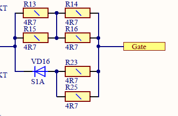
    -About the gate resistance I assume you are referring to the parallel combination of (R13 & R15) as well as (R14 & R16) on the turn-on path and the R23 and R25 on the turn-off path. The advantage from this current configuration may be the fact the external gate resistors will help dissipate power away from the driver. 4 resistors will have better power dissipation capability than a single gate resistance. It looks like you currently have 2.35-Ohms (equivalent resistance of R13 and R15) + 2.35-Ohms (equivalent resistance of R14 and R16) = 4.7-Ohms on the turn-on path (source current) and 2.35-Ohms (equivalent resistance of R23 and R25) on the turn-off path (sink current). Depending on your desired dv/dt at the gate, these values seem reasonable. Alternately depending on your switching frequency (high switching frequency = higher power dissipation within the driver), you may simply choose a single resistance with similar values to save component count and board space.

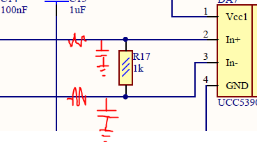
    -With regards to the shorting resistance R17 at the input pins IN+/IN-? Keep in mind the inverting input IN– pulled high internally if left open and the non-inverting input IN+ pulled low internally if left floating. I noticed you mentioned that it is supposed to provide noise immunity in case of long PCB traces, however a small RC filter (Rin<100-Ohms and Cin< 300pF) at either input is generally sufficient to overcome noise on the input stage.

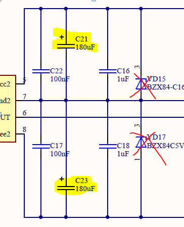
    -You may want to reconsider the values of C23 and C21. 180uF seems excessive to me! I assume you want to get the full 10A drive current, please confirm. Low-ESR or ESL capacitors (4.7uF to 20uF at most) in parallel with C22 and C17 are generally sufficient to adequately bias the driver.
    Additionally, keep in mind the total equivalent gate resistance will impact the drive current regardless how high you pick those bypass capacitors. The higher the impedance on the DRVout path, the lower the drive current (source/sink current) from the driver which will reduce the rise/fall times at the gate. On the flip side, the lower the impedance on the turn-on path, the higher the driver current and higher rise/fall times at the gate and the higher the risk of overshoot (resulting in EMI in your circuit).

    Please let us know if you have further questions or press the green button if you have further questions.

    Regards,

    -Mamadou
  • Thanks for your kind reply.
    1. yeah resistance parallel series is to increase power rating as well as flexibility as i want to change the resistance value to optimize my turn on and off and i want to learn between the analytical method vs actual hardware.
    2. Ron is 4.7 ohm and Roff is 2.35 ohm as you mentioned is right. switching frequency is not too high. it will be around 50 kHz-100 kHz.
    3. yeah RC filter is also shown in the application notes of the ic. is any problem if i only use resistance and its value to be 1k?
    4. the main idea to use 180 uF to so that the capacitor doesn't get discharged with low capacitance value. yeah, its true the peak current depends on the external impedance plus the gate resistance of the device.
    5. so except 180 uF , did the schemtics looks good ?
    6. what would happen if i use big cap like 180 uF vs small cap like 4.7-20 uF.
  • Hi Mohammad,

    It looks like your FETs have a total gate charge of only 17.3nC each which is really not a heavy load to cause full discharge from a 10uF cap (or to require 180uF). Our drivers have been biased with similar capacitance values to drive bigger loads/FETs so the point I am trying to make is that you really do not need that much capacitance. I have not tested our drivers with 180uF to confirm possible issues but you may continue so at your own risk.

    In addition to previous comments, On the layout, I would recommend placing all the decoupling capacitors and clamp diodes as close as possible to the supply pins of the driver and shifting the FETs as close as possible to the driver to reduce PCB trace length and minimize parasitic inductance.

    Other than, your schematic and layout look reasonable.

    Please let us know if you run into trouble with your circuit or if you have further questions.
    Meanwhile, if this addressed your concerns, please press the green button.

    Regards,

    -Mamadou
  • right it has low gate charge but i may need to drive of gate charge around 300-400 nC. i will change the cap to 10 uF or around that value.
    apart from that cap.
    do i need to add any more protection? i don't have an issue with adding more component or size is not a requirement. but i want my PCB robust. it should work even amateur uses it. it should protect from almost everything a user does something wrong which is me.
  • i also want to know about current capability. how to select the isolated power supply for the ic. does using 4 MEA1D1215SC enough to meet the current demand of different ic and proving 10 A sink and source current?
  • is any software where I can see the current capability or transient voltage current of my schematics?
  • Hi Mohammad,

    My apologies for the delayed response.

    We have the simulation tools (unencrypted Pspice model) for this device available on the link below:
    www.ti.com/.../toolssoftware

    For each IC, you will require 2 separate power supplies, one for the primary side VCC1 and the second VCC2. Remember the driver is not sourcing/sinking 10A continuously, that is the peak current at a very specific time (very short duration, usually <1us) of the gate drive turn-on/off transitions.

    Please let us know if you have further questions.

    If not, please press the green button.

    Regards,

    -Mamadou
  • Thanks for you reply,
    1. one of my questions was, is there any need to add more protection in the schematics as i need a robust design for my project.
    2. yeah, i am using one supply for 4 ic i mean same dc supply will be used for all 4 Vcc1,
    3. i am using 4 isolated dc-dc converters to supply VCC2 from same dc supply which is feeding VCC1. is it okay?
    4. the 10 A will be only for turn on and turn off the process which is << switching time i.e <1us as well. that's why i used 3 different capacitor and different type of capacitor with different esr to supply the pulse current.
  • Hi Mohammad,

    1. I reviewed the schematic and your design is very robust. You might be taking too many precautions, actually.

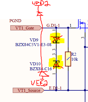
    a. Zener clamps can be regular diode clamps, just with VDD2 clamp from OUT to VDD2. Your circuit will work, but I’ve seen this more commonly in other systems. It also eliminates some of the Zener leakage current.

    b. Gate resistors are sized far bigger than needed. They add more parasitic inductance to your circuit which reduces switching performance. You would probably be able to use one 0805 turn on, and one 0805 turn off resistor. These resistors normally can handle much larger peak current, and should be okay as long as you do not violate their Pdis rating. An example of how to calculate this Pdis is in the datasheet, section 11.2.2. Just change out the internal resistance with the external resistance to ensure it does not overheat.

    c. These caps can be reduced to 10uF ceramics for your current gate charge requirements. Ceramic capacitors can sustain very high peak currents, and most of the peak current will already be supplied by the 100nF caps located close to the IC. 180uF is far too much for almost any gate driver circuit using traditional switches. Also the Zener diodes are unnecessary since you’re already using LDOs to regulate these rail voltages.

    d. Add filter capacitors to inputs. Values can be determined using calculations from the datasheet section 11.2.2.1


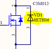
    e. Freewheeling diodes are unnecessary since FETs have body diodes.

    2. One supply should be fine to power all 4 Vcc1 since they are referenced to the same ground.

    3. Using the same VCC1 rail to power the 4 isolated dc-dc converters should be fine, assuming the VCC1 rail can source enough current to power all of these devices.

    4. If you use all ceramic capacitors, these have very low ESR. Their limiting factor is actually ESL, which slows down the possible di/dt of the driver. Ceramics with X5R or X7R dielectric will provide the best performance for our drivers. Please see figure 3 in this application note to see difference in impedance between different capacitor types and packages.

    http://www.ti.com/lit/an/slyt639/slyt639.pdf


    If this helped answer your question, could you please press the green button?

    Thanks and best regards,

    John

  • Thanks for explaining everything. it was so kindful from both of you. :)