This thread has been locked.

If you have a related question, please click the "Ask a related question" button in the top right corner. The newly created question will be automatically linked to this question.

UCC27201A: A question about a spec of Output voltage on HO MAX

Part Number: UCC27201A
Other Parts Discussed in Thread: UCC27201, UCC27200

Hi team,

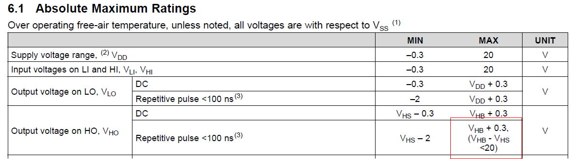
Compared with UCC27201, the datasheet of UCC27201A adds a description of "(VHB-VHS<20)" as below picture shows. Could you please help comments on this. What does this mean? And what we should pay attention to, when using UCC27201A, according to this. Thanks a lot.

Best regards,

Wilson

  • Hello Wilson,

    Thank you for the interest in the UCC27200 and UCC27201A. The note of VHB-VHS < 20V is referring to the HB-HS bias is limited to 20V absolute maximum rating. The HB-HS and VDD to VSS bias voltage range are both limited to the 20V absolute maximum rating. The HO output is limited to the HB + 0.3V if HB-HS is 20V or less.

    I do not think there are any special considerations relating to the HO output range, and the HB to HS voltage range. The driver output to MOSFET layout needs to be short traces with low trace inductance, as recommended in the datasheet Section 10 to minimize driver output overshoot and undershoot.

    Please confirm if this addresses your question, or you can post additional questions on this thread.

    Regards,

    Richard Herring

  • Hi Herring,

    Thanks for your kindly support. I understand HO is an output pin, and its voltage is generated by our part. But there is one more thing need to confirm with you.

    In my customer's design process, they just need to test all the spec in our datasheet. And for HO<HB+0.3V spec, they got below waveform. And we can see a 2.92V voltage peak between HO and HB.

    (Test condition: TDP0500, low voltage differential probe; Test point: HO and HB).

    I assumed the 2.92V voltage peak is due to parasitic inductor of PCB. Is there any risk about this voltage? Will it damage internal circuit of our IC? Or any other issue may cause this voltage peak? Thanks in advance. Look forward your comments about this case. Thanks.

    Best regards,

    Wilson

  • Hello Wilson,

    Thank you for supporting the UCC27201A and the detailed scope plot of the HO waveform. Officially we cannot encourage exceeding the datasheet specification, but there are aspects of this waveform that indicates there would be little stress on the IC due to this very short overshoot spike.

    The duration of the voltage spike is very short, assuming the 2.6ns is the width of the spike. With the parasitic inductance of the board traces, there will be very little time for current to ramp and conduct in the driver internal device body diode. With a voltage spike this short, there will not be significant energy in the voltage spike. And, it is very difficult to record accurate measurements of narrow voltage spikes, some of the amplitude may be due to probe pickup of common mode dV/dt.

    If the customer wants to reduce the spike, place a Schottky diode, 20-30V 1A rating very close to the driver HO and HB pins. This will limit the voltage spike at the IC pins.

    Regards,

    Richard Herring