This thread has been locked.

If you have a related question, please click the "Ask a related question" button in the top right corner. The newly created question will be automatically linked to this question.

UCC28634: AUX Winding Ringing

Part Number: UCC28634


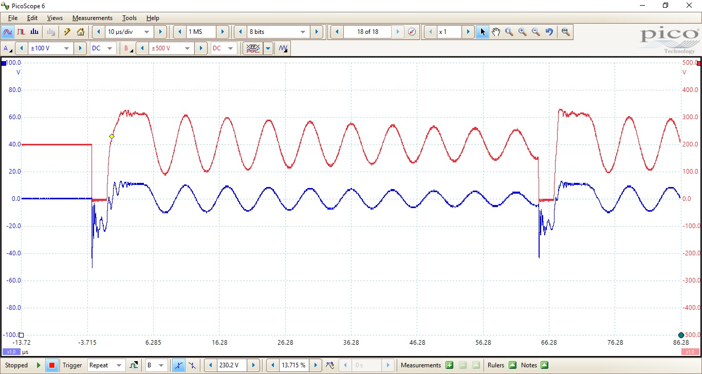
We are designing a high voltage DC-DC flyback converter using the UCC28634 controller. The circuit is currently operational (starts up and somewhat regulates), but is not functioning properly due to excessive ringing on the AUX winding of the transformer during the main switch 'on' phase. This ringing is corrupting the Vsense signal and disrupting the supply regulation. I have attached waveforms of the main switch drain (red trace) and AUX winding (blue trace). Any insight into what may be causing this would be greatly appreciated.

  • Hi Larry,

    Thanks for reaching out. From the waveform, it looks like there is ringing during the MOSFET off time. Could you try snubbing the switch node more? This should help attenuate the ringing on the switch node. This blog post might be helpful for determining snubber parameters:e2e.ti.com/.../calculate-an-r-c-snubber-in-seven-steps

    Best Regards,
    Ben Lough
  • Hello Larry,

    Definitely, the aux waveform should not ring this much during the MOSFET on-time.

    High-voltage transformers usually have more turns than typical low-voltage off-line designs.
    The turns-ratio from primary to auxiliary windings appears to be about 10:1. Since there is a significant overshoot on the aux voltage at the falling edge of the primary voltage, it suggests that the transformer has a lot of leakage inductance on the aux winding that is ringing with the Aux cap for the controller's VDD input. Also the ringing frequency looks like about 1us in period, which may correspond to a reverse recovery time of a standard P-N diode. An ultrafast diode should be used for this application.

    Can you please check the part number of the aux diode and determine if it is a standard-recovery or an ultrafast part?
    If it actually is an ultrafast, then some other source of series or parallel capacitance must be present somewhere in the aux path.
    Can you please provide more details about the auxiliary winding circuit of your application, such as a partial schematic of this portion of your design, plus the transformer parameters?

    Regards,
    Ulrich
  • Hi Ulrich,

    Thanks for your response! The diode used has a 25ns recovery (Diodes Inc. ES1D-13-F) so that seems fast enough. I measured the leakage inductance of the transformer to be ~35uH (shorting AUX and Secondary coils). Below is the AUX supply schematic:

    I was also wondering about the main switch snubber circuit, which I had obtained from another reference design. (Note that the R38 symbol should be a resistor, not a capacitor as shown):

    Also, here is the transformer data sheet. Thanks very much for your help and please let me know if you need any additional information or measurements.

     G194012LF r 0.pdf

  • AUX Supply Circuit:

    Main Snubber Circuit:

  • Hi Larry,

    Thanks for the additional info. Your AUX supply section shows a 1000pF cap C9 across the AUX winding. I recommend to remove that cap and see how the waveform changes.

    I realize that the application schematic of Figure 44 in the UCC28634 datasheet includes such a cap. I think that is a special case that helped clean up some noise in that particular design, but I don't think that it is applicable to all designs. It's value was chosen, in part, based on the transformer inductances of that application. The author(s) probably should have made that clear. After removing it, you can assess your waveforms and determine whether or not you need anything there at all.

    If you think that you do need one, the value for your C9 would be selected to work with your design's transformer.
    I recommend to remove what you have first, and evaluate the results.

    Regards,
    Ulrich
  • Hi Ulrich,

    I removed C9 and unfortunately it did not have a significant affect on the waveform. I have also tried increasing the gate resistor on the main switch to see if that would help the ringing but that has not helped either. Here are the gate drive vs. drain waveforms for reference.

    Regards,

    Larry

  • Hi Larry,

    I'm sorry that the C9 idea didn't work out. But thanks for the new waveform; it provides another clue that might be the answer.
    Given that the MOSFET stays on ~3X longer than the gate drive pulse indicates the primary MOSFET has massive Coss. This Coss can be ringing with the leakage inductance during the extended on-time and even afterward.

    I suggest that your MOSFET may be oversized for the application, maybe by a factor of 3 (for lack of a better number). On-time extension due to Coss is generally unavoidable, but this is an extreme case in my experience. I suggest to try one with 3xRds(on) and 1/3xCoss of what you have now. They may not scale exactly inversely, but the main thing is to significantly reduce Coss. A side effect is that you should see your switching losses go down to make up for the increase in conduction losses.

    Regards,
    Ulrich
  • Hi Ulrich,

    Thanks for your comments! I have tried two FETs so far - one was a GaN device with a Coss = 41pF (TP90H180PS). The other was a traditional FET with a Coss of 140pF (STF20N95K5). Both have yielded similar results. Would anything else be causing the FET to stay on?

    Regards,

    Larry

  • Hi Larry,

    There can be a few things to account for the extended on-time.
    1. Huge Coss in the MOSFET.
    2. More capacitance added to the switched node for EMI suppression or other reasons.
    3. Delay through a gate-drive buffer (if you have one) due to anemic or under-designed drive current available to discharge Vgs of the FET.
    4. Very low peak primary current in that operating condition. (Although simplified, for a flyback it is basically: Ipk/C = dv/dt of the drain voltage, where C is the total capacitance on the switched node.)
    5. Various combinations of any or all of the above.

    The Coss ratings of those MOSFETS are specified at 100V or higher. If you take a look at the Coss curves of each, you’ll see that the STF part exceeds 5000pF for Vds < 5V. The TP part is similar. So the peak current at turn off has to charge up 5nF+ before the Coss drops enough for Vds to really start rising quickly. And the lower the Ipk for that cycle, the slower everything is. In fact Ipk is still rising even as Vds is rising, until Vds > Vbulk. This is worse in the light load condition, of which the waveform appears to be, given the narrow on-time and wide switching period. Not as pronounced at full load.

    Both of these parts have relatively low on-resistance for a 900V+ rating, which makes them quite large MOSFETs. I still suggest to try using smaller devices to see if the on-time ringing abates.

    That is still the main issue to solve: eliminate the on-time ringing. Ringing comes from an undamped L-C tank, either series or parallel. The FET Vds looks solidly on. The AUX reflection of Vds shows ringing, so the L-C tank is more likely to be associated with the AUX winding. (Changing the MOSFET is mainly a shot in the dark.) You removed C9 and it didn’t help. There must be some other reason for the ringing. I request of you to post the schematic of your power stage or enough portion of it to see what other circuits may exist that could contribute to this problem. Also the major parameters (Vin, Vout, Iout) to give it some context.

    Finally, I suggest to scrutinize your prototype to ensure that the parts and connections on the board match those of the schematic diagram. The schematic may work fine, but if the board doesn’t match it, you can have problems. Especially if there exist significant parasitic components not represented on the schematic.

    Regards,
    Ulrich
  • Hi Ulrich,

    Below is the primary side schematic of the converter. Note that there is one error that has been fixed in the layout (R19 is shown connecting directly to R18, but is has been move to connect between R18 and R17). The secondary side is using a synchronous rectifier arrangement. Vin is as shown, secondary side has 2 isolated 32V outputs, both around 0.4A max output.

    Regards,

    Larry

  • Hello Larry,

    I’m sorry that I was unable to reply yesterday. After reviewing your schematic diagram, I don’t see any obvious reason to account for the ringing that you see on the Aux waveform. We already removed C9, which would have been the most likely cause in my opinion. D2 is an ultrafast diode, so that’s not it.

    The only thing left to consider (that I can think of) is that the transformer leakage inductance is ringing with its own winding capacitance. You mentioned earlier that total leakage referred to the primary is ~35uH when all other windings are shorted. Based on ~1us ringing period, this results in Cw = ~724pF. This capacitance seems rather high, but given that this is a high-voltage transformer with high magnetizing inductance, it follows that it has a lot of primary turns, which can have high winding capacitance if wound over multiple layers. If so, such ringing will not show up on the primary voltage which is solidly clamped to GND during the on time and to the switched-node capacitance during the Vds rise time. But it can show up on the AUX winding which is not externally constrained. You may also see ringing on the primary current.

    Is it possible to re-wind a transformer sample using the “bank-winding” method on the primary, which minimizes self-capacitance? Then see if there is any improvement in the Aux waveform?

    Regards,
    Ulrich
  • Hi Ulrich,

    After experimenting with different transistors (which improved things slightly) I went ahead and wound a new transformer with fewer turns than the design from our vendor. This ended up solving the problem (the leakage inductance was about 50% lower) as the AUX ringing was significantly reduced.

    Thanks very much for all your support!

    Best Regards,

    Larry