Hi everyone!
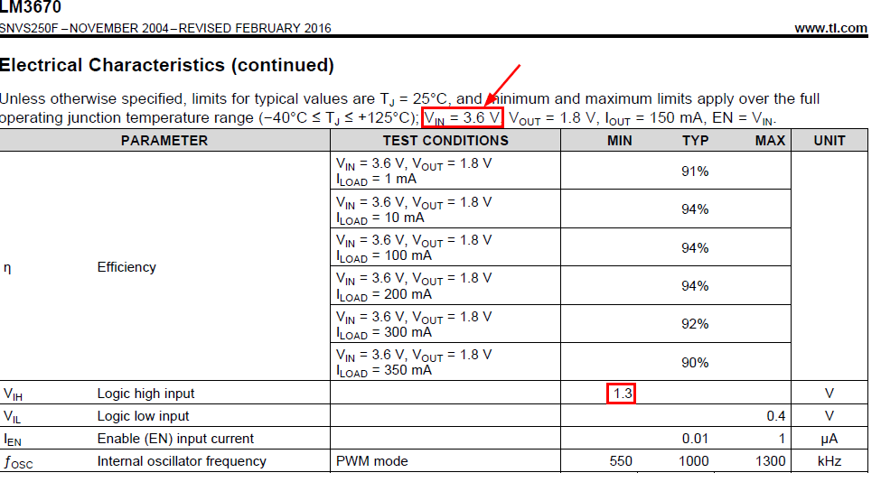
I want to know if the input stage of EN (enable pin) will exhibit an increase in quiescent current consumption if it's voltage is significantly lower than VIN. I have performed an experiment with VIN = 3.6V and EN = 1.5V and this was the threshold where the no-load quiescent current started to get higher. Here is the relevant extract from the datasheet:
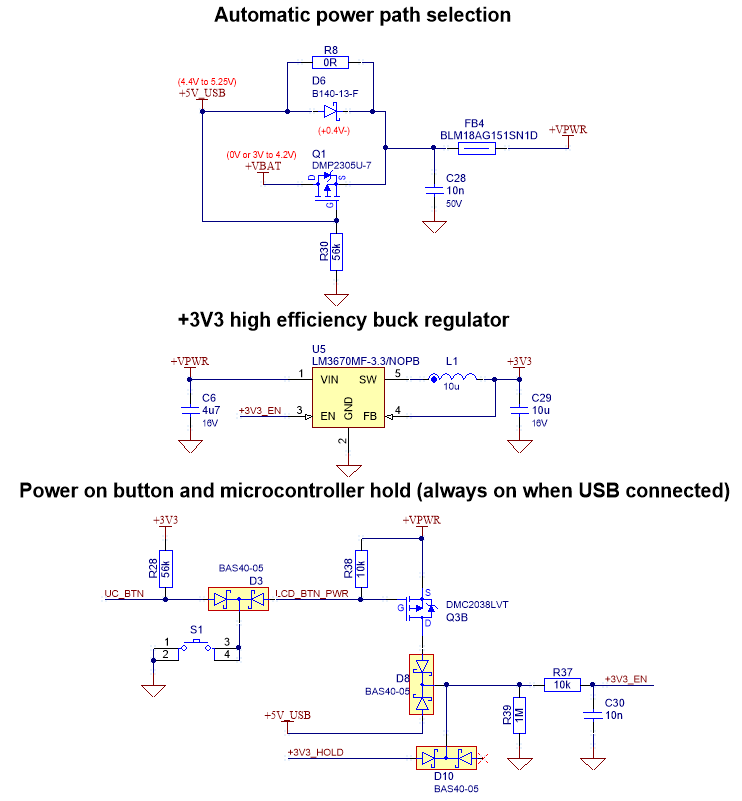
This is what I'm actually trying to do:
I am trying to implement a low cost & low power on/off circuit (suggestions for a better circuit most welcome!). If +5V from USB is connected, regulator must be on. If the button is pressed, regulator must also switch on. In both cases, microcontroller must hold the regulator enabled via a GPIO output pin connected to net "+3V3_HOLD". When the microcontroller wants to switch off, it takes +3V3_HOLD low.
+VBAT is connected to a LiPo battery (+3.6V to +4.2V). So when the circuit runs from battery, U5-1 (VIN) = ~4.2V, but U5-3 (EN) = ~3.1V (schottky diode drop over D10). This is a difference of ~1.1V. The datasheet specifies EN Vih threshold for VIN=3.6V, but not for VIN=4.2V and this raises my question regarding the EN pin input stage:
Is the EN pin a regular complementary PMOS - NMOS pair with higher shootthrough current if the gate voltages are in the middle of the supply voltage? Or is it a special circuit that exhibits very low leakage current?
Will my circuit perform well with minimum quiescent current or is there a better alternative?
Thanks in advance,
Pieter


