


Other Parts Discussed in Thread: TLV62130, TPS62135, TPS82130, TPS62230, LMZ21701, TPS62821
Hello,
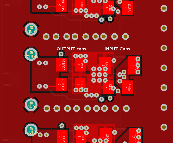
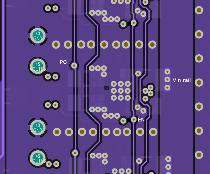
du to some size constraints, fitting all the components on the same side of the board like on the reference layout was a bit difficult: since we need 6 different rails I was concerned that different converters would be too close to each other and start to interact (VOS or feedback picking switching noise from nearby converter).
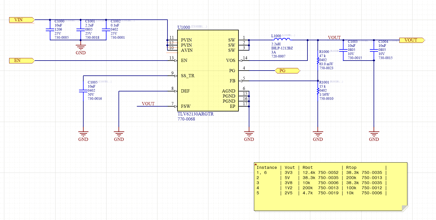
I did follow the layout guidelines of the datasheet though. All rails are layed out the same way. Only feedback resistors values change.
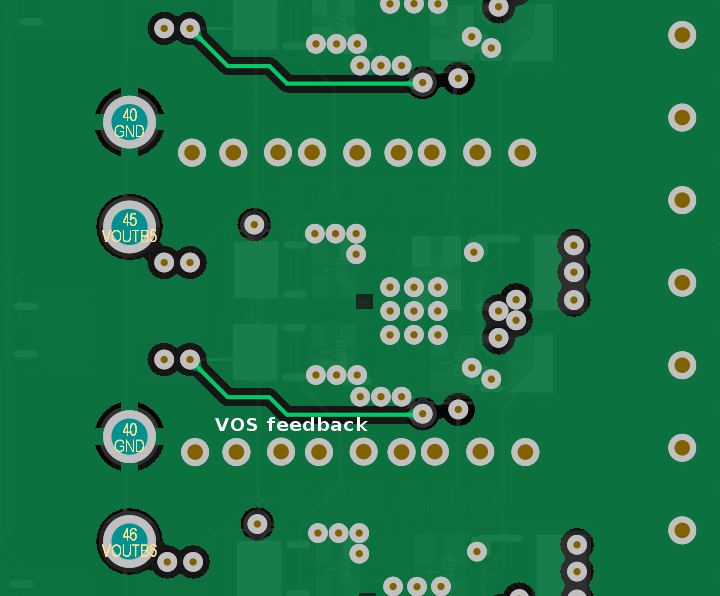
Special care has been taken to have short current loops, and as may solid GND planes as possible, especially below the IC and over the VOS line.
This layout is similar to other power supplies we already successfully designed with other converters, but I don't know if there are some reason it would not work with the TLV62130. Do TI know of some similar designs working on the field?
Feedback would be much appreciated befor we launch that in production!
Input voltage : 6V (if powered via battery) to 12V (if powered from an isolated DC/DC)
Output voltages: 5V, 3.8V, 3.3V, 2.5V or 1.2V depending on the rail
Output currents: from ~100mA (3.3V, 2.5V and 1.2V rail) to 2.8A (3.8V and 5V)
schematics:
Top layer : input and output caps
VSYS is the input voltage
VOUT* are the output rails
Internal layer 1 : VOS and GND plane
Internal 2: GND plane
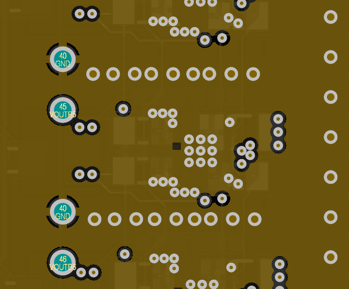
Internal 3: GND plane and ENable / PGood signals
Internal 4: GND plane
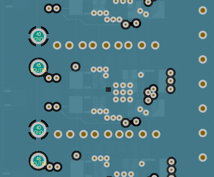
Bottom: IC, inductor, feedback resistors, SS cap, 0.1uF input cap


