This thread has been locked.

If you have a related question, please click the "Ask a related question" button in the top right corner. The newly created question will be automatically linked to this question.

LM43603-Q1: About Thermal Vias under DAP

Part Number: LM43603-Q1

HI Team

If the bottom pad of the LM43603-Q1 is not soldered properly, it is found that the output voltage is abnormal.

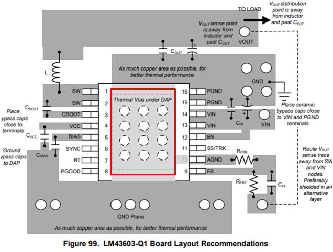
We have designed six vias in the bottom pad as shown in the datasheet.

However, in the SMT process, we found that lead leaked through the vias.

I would like to ask you some questions about this issue.

1. Why is the voltage unstable when the bottom pad is not properly soldered?

2. What percentage of the bottom pad area should be soldered for stable output?

3. What is the purpose of Vias in bottom pad? (Heat dissipation, GND strengthening, EMC enhancement, etc)

4. We are going to reduce Via of bottom pad from 6ea to 4ea.(System Spec : 12Vin -> 3.3Vout / 2A)

    Is there any problem in reducing Via?

5. Is there a formula for calculating the number of vias required for a bottom pad?

    If yes, please share it.

Thank you.

  • The DAP on the device is part of the electrical and the thermal circuit for the device.

    The DAP provides a solid electrical ground connection to the substrate of the die.

    The DAP also provides a very good thermal path for the internal power of the device

    to flow to the ambient.

    As long as there is some electrical conneciont from the DAP to ground, that should be sufficient.

    Reducing the number of vias will increase the thermal resistance from junction to ambient and

    may result in an increase in the die temperature.  

    It is difficult to predict the exact change in thermal performance when changing the number of

    vias, however the following Application Note should be of some help.

  • Hi Charles,

    1) The voltage could go unstable because internally the PGND and AGND are not connected in the IC. The PAD is where AGND and PGND should be connected, therefore you have a better noise immunity especially at higher current and frequency. 

    2) Ideally is 100% coverage, i would say greater than 90% solder coverage should be ok

    3) The main purpose of VIA in bottom pad is for heat dissipation to be spread out in other layers such as bottom layer. 

    4) I think that should be ok. In our EVM we use 5 vias. http://www.ti.com/lit/ug/snvu388/snvu388.pdf

    5) There is no exact formula to calculate the number of vias required for bottom pad. What we have is only guidelines based on example layout on PCB or EVM to get a thermal performance from a specific package. We also have the recommended stencil for solder paste at the end of the datasheet. 

    Here is some useful information on Power PAD http://www.ti.com/lit/an/slma002h/slma002h.pdf

    In general we tend to use a via with a hole diameter of 8mil and a via diameter 22 mil. 

    Thanks and i hope that helps

    -Arief