This thread has been locked.

If you have a related question, please click the "Ask a related question" button in the top right corner. The newly created question will be automatically linked to this question.

TPS546C23: Power management forum

Part Number: TPS546C23

TPS546C23 P3V3.pdfhttps://e2e.ti.com/cfs-file/__key/communityserver-discussions-components-files/196/tps546c23.7zHi, 

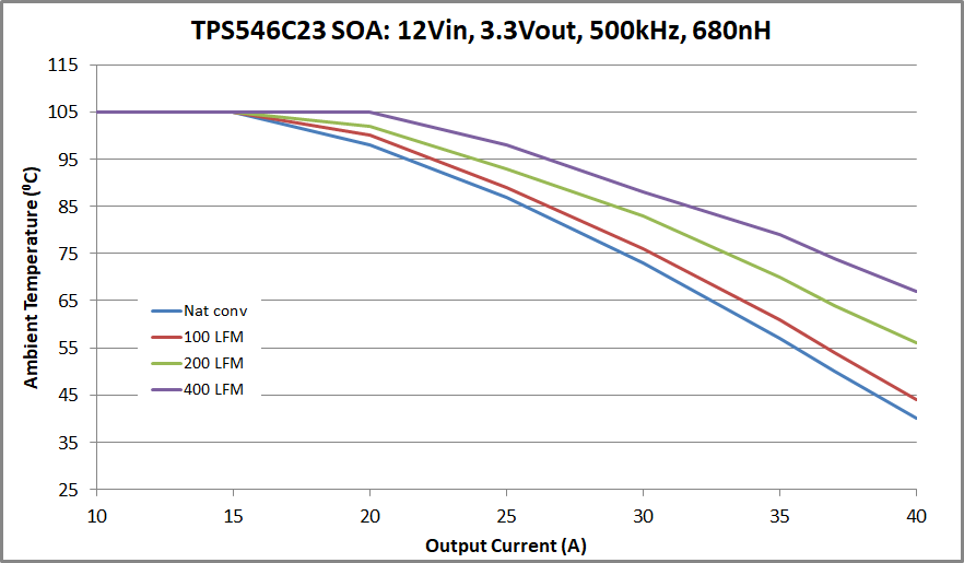
Customer wants to achieve 12V to 3.3V/30A application with one pcs TPS546C23. 

Here is the spec and schematic. Customer wants to know the recommended Pmax for this part and confirm if there are risks for this application.

Can you help to check the schematic and give some comments? Thanks a lot. 

Parameter

Spec

Vin(V)

12

Vout(V)

3.3

Imax(A)

30

TDC(A)

30

Icc Dynamic(A)

15

Rise di/dt(A/uS)

2.5

Fall di/dt(A/uS)

2.5

DC/AC Voltage regulation(%)

±5

Oliver Ou

  • Hi Oliver,

    Please see my feedback below:

    • AGND and PGND should be tied together and connected directly to the thermal pad in order to minimize noise.  It may be necessary to explicitly state this on the schematic depending upon the customer's schematic/layout conventions.

    • DRGND and PGND should be tied together and connected directly to the thermal pad, in order to minimize noise.  This may be necessary depending upon the customer's schematic to layout convention.

    • It is recommended to have BP6 tied to the thermal pad (PGND) with a 100 nF or larger capacitor, placed as close as possible to the BP6 pin, in order to stabilize the internal LDO.  A low impedance path for this trace is critical.

    • Locate C2793, the 3.3 nF capacitor from PVIN to PGND as close as possible to the the PVIN pins.  This capacitor can be placed on underside of the PCB, if this helps to reduce the total trace length of mounting on the same side as the TPS546C23 device.

    • RSN should be connected to ground at the load, similar to RSP.  It may be necessary to show this routing explicitly on the schematic in order to ensure proper layout.

    • I show placeholders for the snubber network which is fine, I would suggest though that if you use a snubber network that you use a resistor with a minimum power rating of 1/4 W.  This will allow for 1/2 derating based on: C*V­2*FSW.

    Thanks,

  • Hi Ryan,

    Thanks a lot for your comments.

    Can one pcs TPS564C23 can support 3.3V/30A output? Customer concerns the thermal issue.

    Do you have an derating curve for 12V to 3.3V? that would be a good reference.

    Thanks,

    Oliver Ou

  • Hi Oliver,

    Please see the Safe Operating Area (SOA) Curve listed below:

    Previously the TPS546C23 device was tested on the EVM in accordance to the: "Method of Graphing Safe Operating Area (SOA) Curves in DC-DC Converter" report HERE.  At 30A or below, with the parameters listed in the title of the graph above: Vin: 12V, Vout: 3.3V, Fsw: 500kHz, L: 680nH, the TPS546C23 device was found to be within the safe operating range when operating with an ambient temperature of 105degC.

    Thanks,

  • Hi Ryan,

    Here is the SOA curve for 12V to 1V output listed on datasheet. It seems it even bad than 12V to 3.3V output.

    if the datasheet is right,  the 12V to 3.3V SOA curve should have issue. 

    Can you help to check again?

    Thanks.

  • Hi Oliver,

    I am looking into this now, and will follow up by Friday (6/14).

    Thanks,

  • Hi Oliver,

    I am continuing to work to determine device settings used during the datasheet SOA curves.  I will report back as soon as I find this out.

    Thanks,

  • Hi Oliver,

    I will close this out the week of 7/8.  Thank you for your patience.

    Thanks,

  • Hi Oliver,

    Please see the SOA curves listed below for this application.  This is based on the proper data set for this condition.

    Thanks,