This thread has been locked.

If you have a related question, please click the "Ask a related question" button in the top right corner. The newly created question will be automatically linked to this question.

LP8863-Q1: I2C register writing problem after power up

Part Number: LP8863-Q1

Hi team,

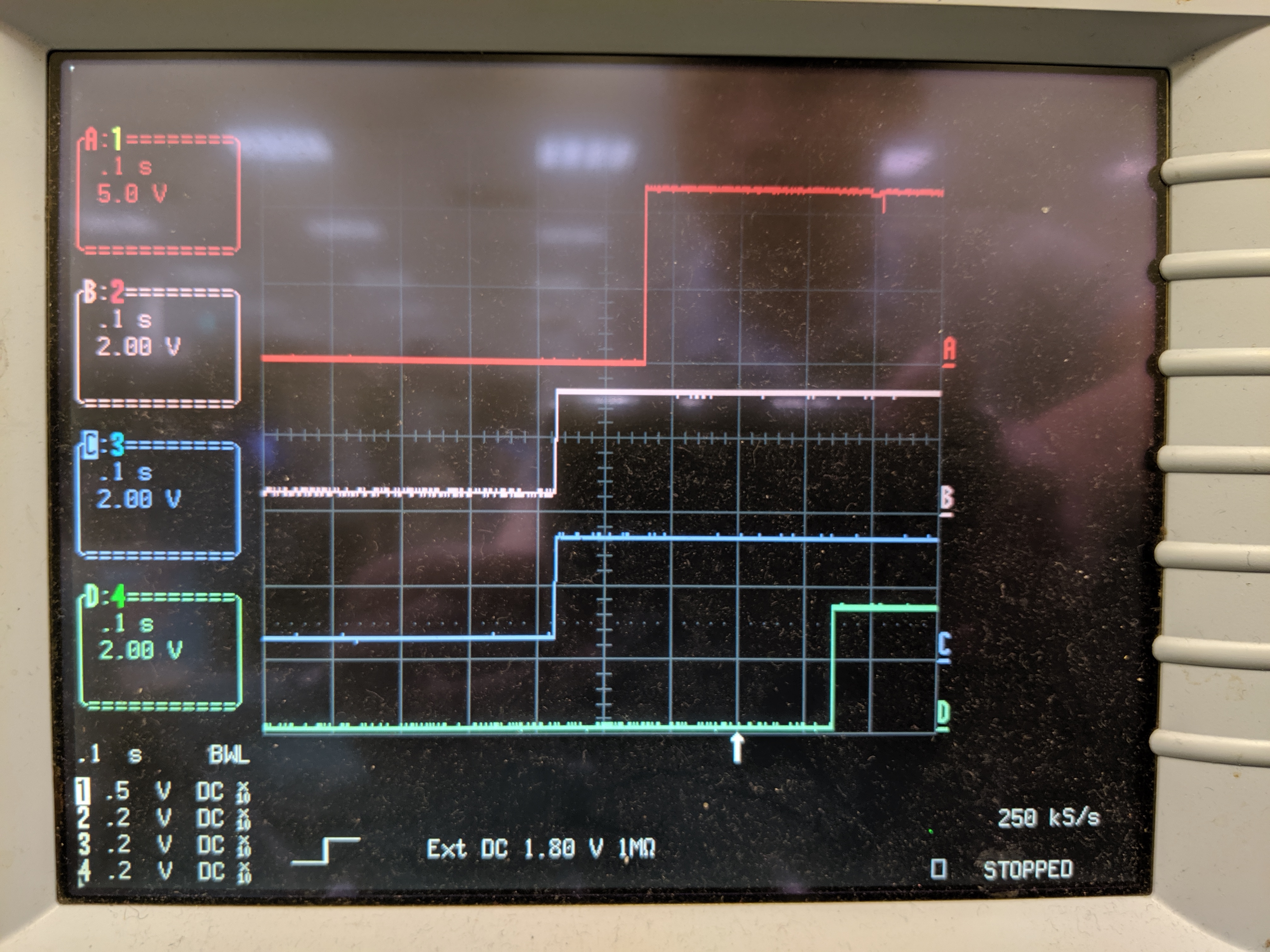
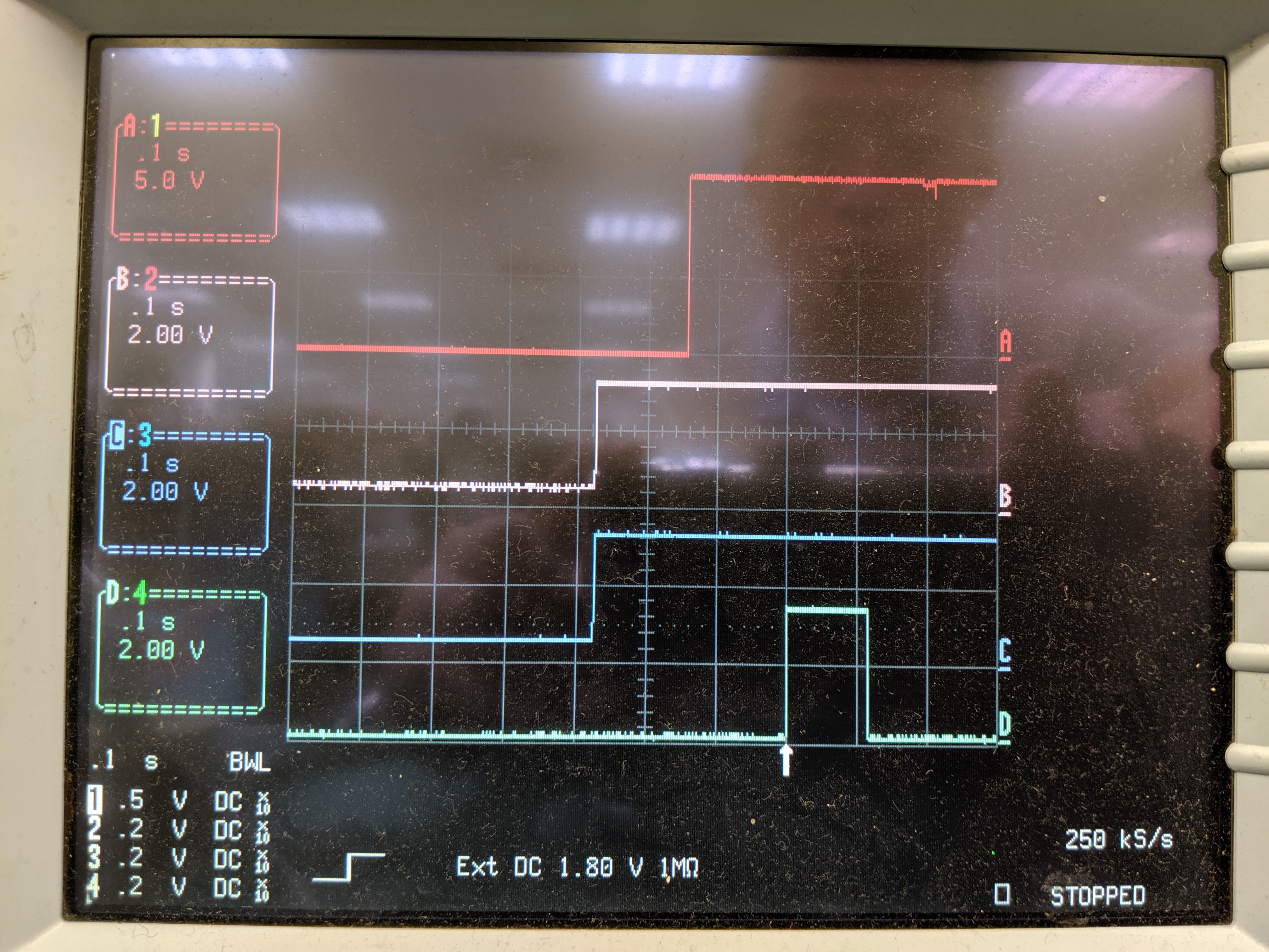
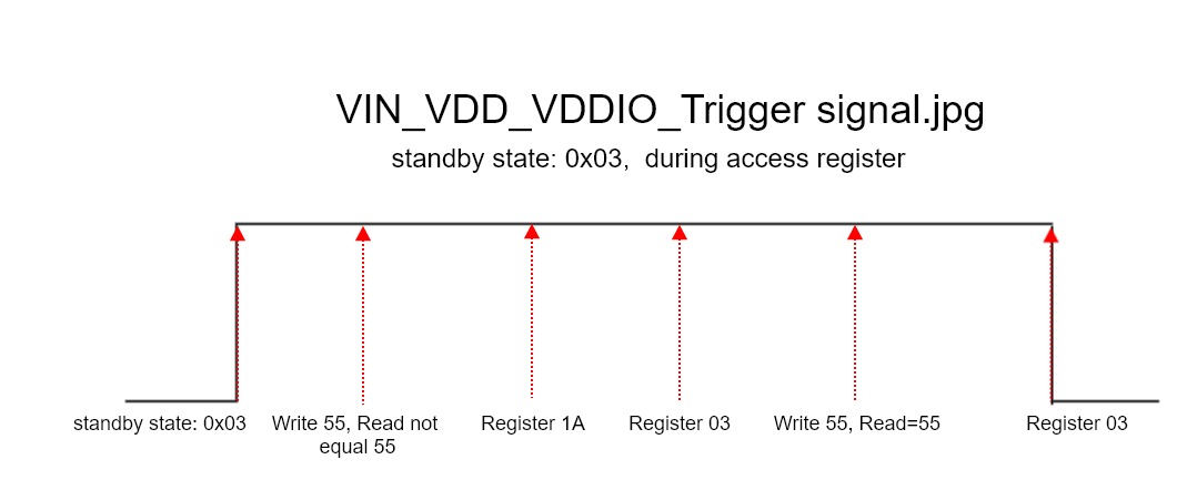
We face a problem regards to LP8863 I2C writing after power up. Refer to datasheet description, register can be access when it shows in standby state. 

When power up LP8863, we make sure FSM_LIVE_STATUS shows 0x03. Then write to register address 0x28 with 0x5a5a, and then read it back. It shows 0x0303 which is different with what we write. 

We then monitor the FSM_LIVE_STATUS after power up, it shows 0x03 -> 0x1A -> 0x03. The writing problem only happen at first time 0x03, and normal after second 0x03. 

Would you please check what is the reason cause this problem. We would like to know when is the proper time to access LP8863 after system power up?

Thanks!

Regards,

Alex

  • Hi Alex,

    When you say "power up", what is the power up sequence? Could you show the power up sequence of VDD, VDDIO, VIN, and when you start to write the registers? 

    Since the readback of address 0x28 is not right. The readback of FSM_LIVE_STATUS may also not be right. That is to say, although the FSM_LIVE_STATUS shows 0x03, we can't make sure it's in standby mode.

  • Hi Shirley,

    Your comment is a bit contradictory, when the  FSM_LIVE_STATUS shows standby state, it should means LP8863 ready to access without problem/error, if it not ready, it should show something else. Not to show standby.

    I am confirming the power up sequence, will update later.

    Thanks,

    Alex

  • Hi, Shirley :

    I'm sorry to jump into your communication firstly.

    Here comes power up sequence waveform. please check it and advise if you have any finding ...

    VIN_VDD_VDDIO_Enable Siganl.jpg  =>

    Ch 1: VIN,  CH2: VDD,  CH3: VDDIO,  CH4: Enable (pin)


    VIN_VDD_VDDIO_Trigger signal.jpg =>

    Ch 1: VIN,  CH2: VDD,  CH3: VDDIO,  CH4: Trigger (standby state: 0x03,  during access register)

    Thanks

    CD

  • Hi CD,

    Thanks for the sequence waveform. The power on sequence looks ok. Could you point out at which particular time in the waveform did you write the register? And when are the three particular moments that you read the FSM_LIVE_STATUS register to be 0x03, 0x1A, and 0x03? It's quite strange to see the readback to be 0x1A, which is not a normal value that the device can feedback.

  • Hi, Shirley :

    We added the access timing in the sequence waveform.

    Please check it and feedback your comments if you have any finding ...

    Regards

    CD

  • Hi CD,

    Sorry we still can't figure out the reason and we can't replicate this issue on our board yet. Can you confirm this behavior happens with every device, or happens at just one device?

    I'm not familiar with the oscilloscope that you use. What is the time base in your waveform? 1s/Div or 100ms/Div?

    Besides that, may I ask what is the purpose of writing the brightness code before EN is active?

  • Hi, Shirley :

    Due to functional safety concern, we have to make sure I2C communicaiton can work normally before enable pin is active.

    This is we would write a certain value via I2C and then, readback to comapre its consistency (equal).

    After that, we would start to control LED driver (LP8863).

    As for we got the wrong value after sandby of LP8863, we found it's our software I2C read (function) bug.

    and our software member fixed it immedately.

    It seems everything goes well now.

    I'm sorry to bother you ...

    Regards

    CD

  • Hi Shirley,

    Per following this issue with RD, they figured out there is something wrong with the coding of I2C reading process. After correcting the problem, there is no problem now. We can close this thread.

    Thanks! 

    Regards,

    Alex