


Team,
The use case is:
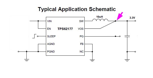
TPS62177 is powered off as there are no VIN source.
However an other power source provide 3.3V to the TPS62177 SW and VOS pins (see pink arrow on picture below).
I assume that the SW output and VOS input are not fail-safe pins.
-What would be the effect on input and output pins? and are the effect the same on both input/output?
-Does it affect the long term reliability?
-What do you advise in such case (how to protect INPUT/OUTPUT pins, acceptable period of time that INPUT/OUTPUT pins can see a voltage,..etc)?
-Any existing TI reference design that shows protection for this use case?
Thanks in advance,
A.

