This thread has been locked.

If you have a related question, please click the "Ask a related question" button in the top right corner. The newly created question will be automatically linked to this question.

UCC28C40: UCC28C40- output waveform anomaly issue

Part Number: UCC28C40

Hi Team:

RD feedback when Vin_min Vgs waveform anomaly and Vin_max is normal as attached.

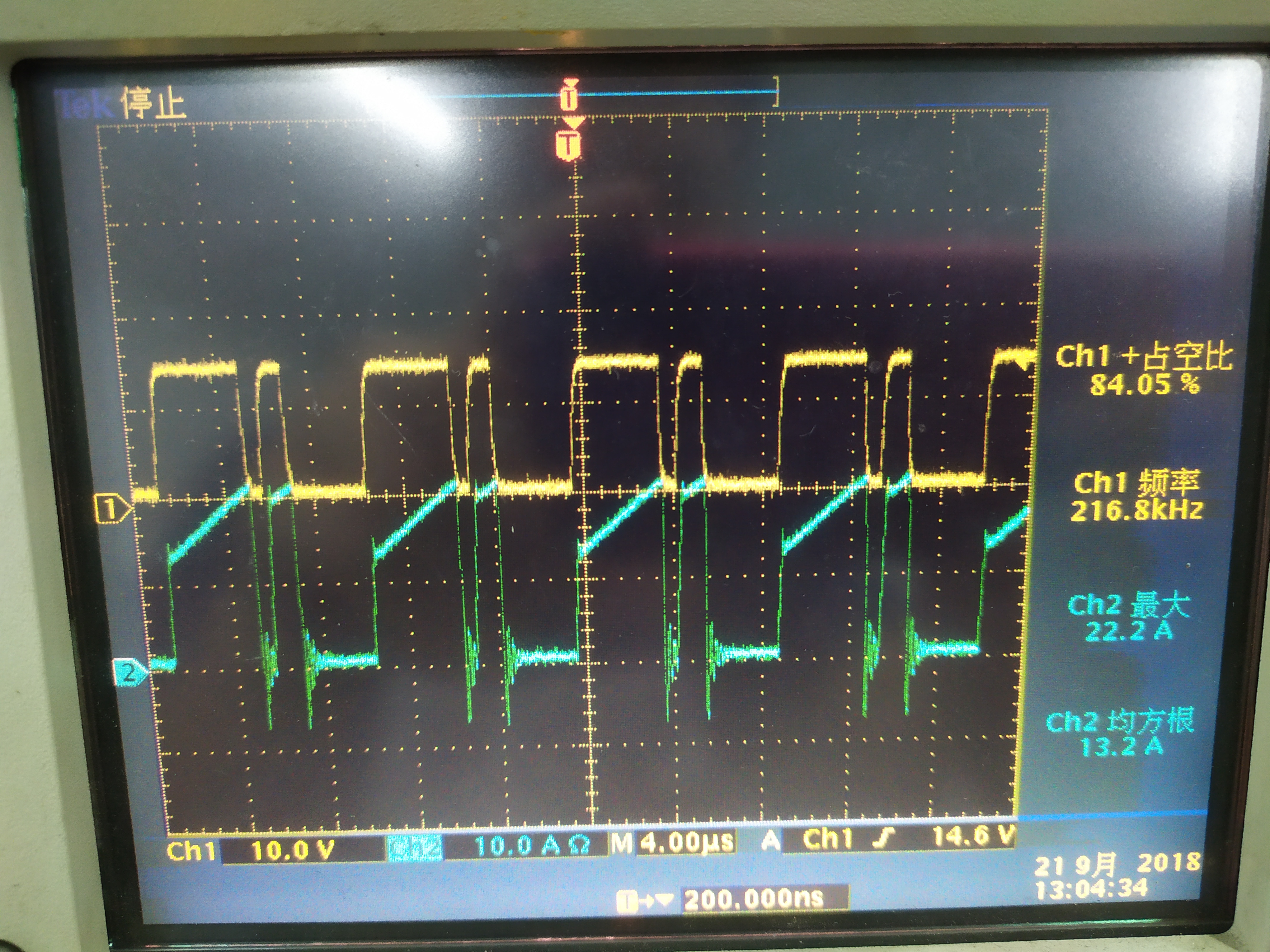
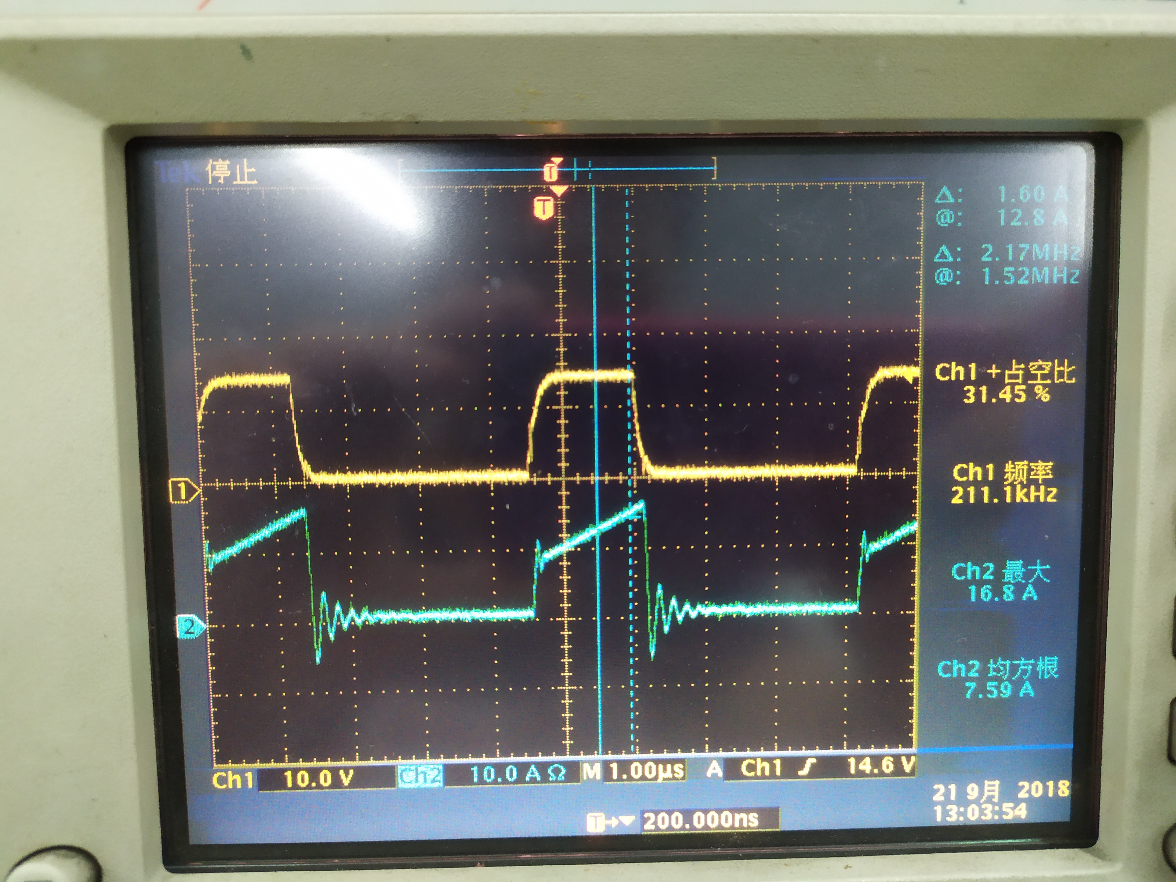
Pls help to confirm ~ what's issue may cause Vgs waveform anomaly ? (setup issue ? layout issue?)

Condition:

Vin_min=13V , Vin_max=24V

Vout=12V , Iout=6A

turns ratio=3:6

Lp=800nH

Rg=10 ohm

Could you share layout guidelines for reference ?

As I check , RD use double layer PCB and two trace parallel of OUT & CS as green line as below 

will it cause Vgs anomaly ?


thanks.

Regards / Mark

  • Hello Mark

    This could be a sub-harmonic oscillation due to operating at D > 50%. If Vo is 13 and Vi is 12 then D would be (Vin*Ns)/(Vout*Np) = (13*3)/(6/12) = 54%.

    At 24Vin I calculate a duty cycle of (13*3)/(6/24) = 27% which is consistent with the 30% I get from reading the 'stable' plot.

    I'd suggest a check of this by verifying stable operation at lower duty cycles - the system may become partially unstable as D increases towards 50%.

    The solution is to add slope compensation network such as that shown on Fig 27 of the data sheet or to avoid operation at D > 50% by changing the transformer turns ratio. Note that although operation at D > 50% is unstable the boundary between stable and unstable operation isn't sharp. Typically operation at D < 40% will be stable with reducing stability margins as D increases towards 50%.

    Running a gate drive line parallel to the current sense line is always a bad idea because the high dv/dt rate on the gate drive signal can couple noise onto CS.

    The CS filter components should be located AT the IC for best filtering effect.

    I'd also suggest that the 10k resistor from gate to source should be moved to the ground end of the current sense resistor - this will slightly reduce the noise at the CS resistor so I wouldn't do it unless there is a re-layout planned.

    I don't understand the function of the diode across the CS resistor - please make sure that it does not clamp the voltage appearing at the CS resistor because if it does the controller won't be able to properly control the PSU.

    Regards

    Colin