This thread has been locked.

If you have a related question, please click the "Ask a related question" button in the top right corner. The newly created question will be automatically linked to this question.

TPS54672: Sink capability of TPS54672

Part Number: TPS54672
Other Parts Discussed in Thread: TPSM846C23

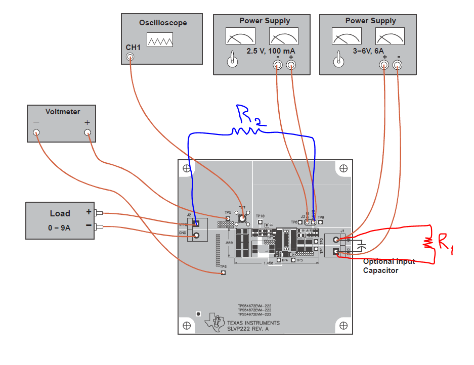
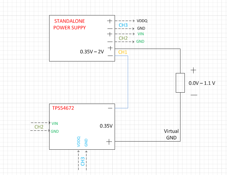
I would like to use TPS54672 to sink continuously changing current at a certain voltage so that it can act as active load. I wanted to test before I go further and design the circuit. I got the EVM and build my circuit on breadboard. Before I power it up I want to make sure the following part I found the EVM user guide. 

" To sink current, increase the current capacity of the 2.5-V supply, and connect a load resistor between the positive load terminal and the positive terminal of the 2.5-V supply. "

I do not really get why I need to put that load resistor first. If I need such load resistor what should be value? Is it really supposed to be connected between VTTQ and VDDQ pins?

Thanks for response in advance...

  • Hi Fatih, 

    When TPS54672 sink current, the inductor current is negative. 

    When high-side FET is on, the inductor negative current will charge input cap and make Vin rises up and eventually damage the part. 

    To prevent this happening, you have to add a load at Vin. 

    Basically you can not use this part as a load circuit you want.

    Thanks

    Qian

  • Hi Qian,

    I would like to thank you first for your prompt reply. 

    You stated that I cannot use TPS54672 as active load but when the TPS54672 sinks current at a constant output voltage it will act as active load right? 

    You also stated that I should connect a load between VIN and GND if I want to sink continuous current. But, the EVM user guide states the following: 

    " To sink current, increase the current capacity of the 2.5-V supply, and connect a load resistor between the positive load terminal and the positive terminal of the 2.5-V supply. " Please refer to Fig. 2-1. Connection Diagram in USER GUIDE.

    My understanding is from the sentence above is that I should connect the load between VTTQ and VDDQ pins?

    Could you also please let me know which resistance (R1 or R2 in picture below) I should use and what should be its approximate resistance value?.

    Thanks a lot... 

  • Hi Qian,

    I think I should give you a bit more details about the circuit that I am trying to design. I need to control the output voltage of a power supply commanding through a processor. I want that power supply to give me output voltage varying from 0V to 1.1 V and 3A max. After a quick search I found TPSM846C23 but the problem here is that the minimum output voltage that you can go down with this power supply is 0.35V. So I decided to create an virtual GND starting at a certain votlage as you can see the block diagram.

    As the first solution, I picked TPS54672 since it can source and sink current at 6A max at a constant voltage. Setting the output voltage of the TPS54672 to 0.9 V and setting the minimum output voltage of TPSM846C23 the voltage across the load will span from 0.0V to up to 1.1V, which is exactly what I want. I am at the stage of testing the circuit with the EVMs of this two power supplies. 

    Another solution is to use a diode which will induce forward voltage drop when it forward biased. So, I picked a diode which has minimum voltage drop of 0.35V so that I can span the load voltage from 0V to 1.1V adjusting the VDCCOMMAND from a closed loop control implemented into the processor as you can see from the block diagram below. But that solution looked to me a bit more complex than the other one since it needs closed loop control since to the forward voltage of the diode is not constant as the case in the first solution. I just wanted to give more details to see if you can suggest something else. THANKS...


  • Hi Fatih, 

    Thanks for the additional information. 

    If you want to test TPS54672 alone, I suggest to add a load between VIN and ground to prevent Cin being charged up by negative inductor current. 

    I'm pretty sure this method works because I always use this method to test the part at sink current mode. 

    Adding a load resistor between the positive load terminal and the positive terminal of the 2.5-V supply may work as well, but I did not try it before. 

    In your real system, because TPS54672 and TPSM846C23 share the same 5Vin, the load resistor between VIN and ground (or between VIN and Vout) may not needed, because the TPS54672 negative current will be consumed by TPSM846C23. 

    Thanks

    Qian

  • Hi Qian, 

    Ok then I will connect the load between VIN and ground to prevent Cin being charged up by negative inductor current. Is there any suggestion regardign the value of that load since it will consume power from 5V source continuously. Would 10 kohm be fine?

    One more concern regarding TPS54672. The accuracy of voltage drop across the load is important for us. So, having a stable virtual GND is a key point. But, here is what I have seen from the USER GUIDE of TPS54672EVM. As you can see below when it changes to sink current mode there is almost 15mV shift at the output voltage. Well, the current jumps from 3 to -3 A but in my case it will be from 0 to -3 A so I am not expecting that much votlage shift but I would prefer not to have any. Do you have any suggestion to solve that issue. 

    Another thing is that once I prove the concept I will change TPS54672 with another one that has constant output voltage. Is there any TPS series power supply that can give stable constant output. The output can be any value from 0.35 V up to 1.2V. Thanks...

    THANKS...

  • Hi Qian, 

    Here is the initial results of my test. The diagram below shows the test setup I have. I used the standalone power supply initially rather than using TPSM846C23 since I want to check the performance of sink unit first. All channels on the standalone power supply are isolated from each other. 

    As you can see from the last picture showing the volage and currents at each channel although I set the CH2 (VIN for  TPS54672  ) to  5V it goes above it because of the negative inductor current as you also indicated. But, this 10 kOhm resistance across the VIN and GND did not look to me helping since as I increase the voltage at CH3 (TPSM846C23 ) the voltage at CH2 goes higher and higher... I could not further test it at higher current since is will exceed 7V at Ch2 and damage the deicve. Any suggestion for that...Thanks...

  • Hi  Fatih, 

    10k ohm is too large. The negative current could be up to 3A based on the information on your diagram. 

    The load current on 5Vin should be larger than 3A*0.35V/5V=0.21A. 

    If you have electronic load, I suggest to use electronic load to add  a load current larger than 0.21A on 5Vin.

    To be safe, you can add a current much higher 0.21A.

    Thanks

    Qian