


Other Parts Discussed in Thread: TPS63020
Hello,
I have a design that uses two TPS63020's to generate 5V and 3.3V. The units seem to test out fine when I build and bench test them; but my client has had several units "spontaneously" fail in the field under different set of circumstances, but in all cases the TPS63020 has failed with the device "getting hot". I am in the process of recalling the failed units for analysis. In the meanwhile, I would like to tee up a review of the design.
The 5V section schematic is as follows (the 3.3V is the same except for the feedback ratio):

The load is not particularly demanding -- in most cases, well below 100 mA -- but the design in intended to allow for up to 1A.
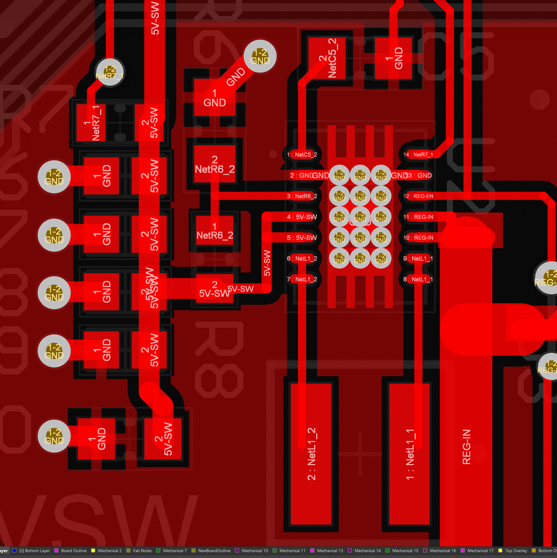
Looking at the layout, I see that I could fatten up the inductor and output traces a bit (and also straighten the exit path out of the Vout pins), but pretty much everything is a short distance to the regulator. Not shown in the schematic clipping above, but visible in the layout is a 10uF ceramic cap on the input Reg-In rail.


In the very first version of the product, we had the possibility of Vin exceeding 7 volts under certain conditions. However, we put a clamp on the input side to limit that to 6.5V or less. When the regulator is enabled, the input rails will drop to the nominal 3.7V (battery) or 5V (USB) depending on what power source is connected.
There is also a possibility that a inductive load may be kicking back excessive voltage to the output rail. That is still being investigated.
Thank in advance for your help on this!


