This thread has been locked.

If you have a related question, please click the "Ask a related question" button in the top right corner. The newly created question will be automatically linked to this question.

TPS61252: TPS61252 High Shutdown Current - Please Help

Part Number: TPS61252

After working with a new prototype for 15-30 minutes or more, the shutdown current starts to rise. At first, it was ~1uA, then it was 40uA, then it continued to climb and now it is consuming 4 mA in shutdown mode. This is the second prototype that exhibits this type of behavior. The first prototype was as high as 10 mA shutdown current and pretty much stayed around there. I went so far as to remove every component from the prototype, leaving just the TPS61252, in order to determine that it was the source of the current draw.

I can think of a few things in my design that can be improved but I allowed them so that I could more easily fit components in the available space. I never suspected that making these compromises might cause a shutdown current malfunction. Can someone please evaluate my design and tell me if a glaring error is discovered.

Here is the schematic:

I measured voltages while the device is in shutdown:

  • Pin 1 (GND): 0V
  • Pin 2 (VOUT): 0V
  • Pin 3 (FB): 0V
  • Pin 4 (ILIM): 0V
  • Pin 5 (PG): 0V / floating
  • Pin 6 (EN): 0V
  • Pin 7 (SW): 3.52V
  • Pin 8 (VIN): 3.52V

I also removed the inductor so that Pin 7 is not connected and this did not solve the problem. So the leakage current is coming from Pin 8.

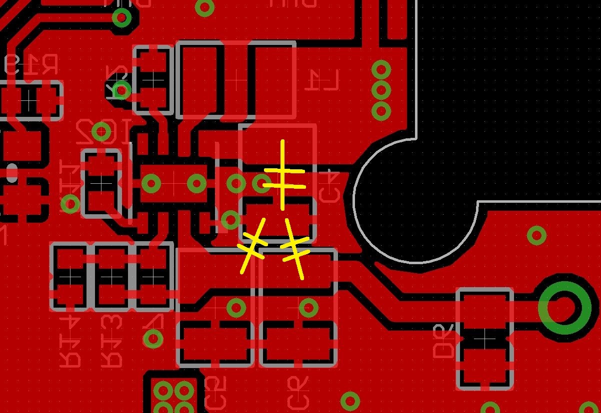
I don't think that the schematic has any issues. It must be the layout. My biggest mistake (probably) is the PCB stack-up. It has 4 layers with a ground plane and a power plane. The power plane is directly beneath the TPS61252, not the ground plane. Also, the footprint contains thermals which "choke" the ground pour a bit, potentially causing more issues with the ground path.

Here is a picture (mirrored because it is a top-view of the bottom layer):

I can send gerber files if needed.

About to receive a third prototype tomorrow that I can test. If you have any recommended steps to test this prototype, please advise.

Regards,

Seth Berggren

  • Hi Seth,

    it seem the device is damaged. 

    when you receive the new prototype, measure the shutdown current firstly before enable the IC.

    what the part number of the inductor? make sure the inductor current is high enough

    please rotate one of the output capacitor (C5, C6) 180 degree, to minimize the loop between the IC and output capacitor.

    enable the device after finishing the above suggestions

  • Thanks for your response Jasper. The inductor part number is: DFE201610P-1R5M=P2. I will check to see if the prototype manufacturer swapped it for another part as they did with some other components.

    I also thought maybe programming of the prototype could cause the EN pin of the TPS61252 to get cycled at a high frequency. Might it be necessary to put a LPF on the Enable pin?

  • the inductor is good. 

    yes, please add LPF on the enable pin. I hope we can find the moment when the device got damaged. then it is easier to find the root cause.

  • For now, I have the device modifications all made except for the LPF. The MCU GPIO that controls the EN is disconnected and there is a pull-down resistor instead. I am getting 3.67 uA current draw total. My other device, with the TPS61252 removed, measures ~2.50 uA total. We can assume the TPS61252 is drawing around ~1.0 uA. I'm going to let it run overnight (bed time for me) and check it again tomorrow morning to make sure nothing has changed.

    Also, instead of turning the capacitor around, I had some 22 uF 10V 0603 capacitors on hand. So I was able to increase capacitance and get shorter path by soldering like so:

    Tomorrow I will implement the LPF and begin testing TPS61252 in it's active mode.

    Thanks again for the assistance.

  • Hi

    any update on this issue? i will closed the post if the issue is solved.