This thread has been locked.

If you have a related question, please click the "Ask a related question" button in the top right corner. The newly created question will be automatically linked to this question.

LM5122: LM5122 unexpected hiccup overload

Part Number: LM5122

I have a problem with a boost converter based on the LM5122 and hope somebody could help me finding the cause.

The hiccup overload protection operates when the load becomes higher than ~600mA.

Design made using Webench
Vin [18V - 22V]
Vout 24V 8A

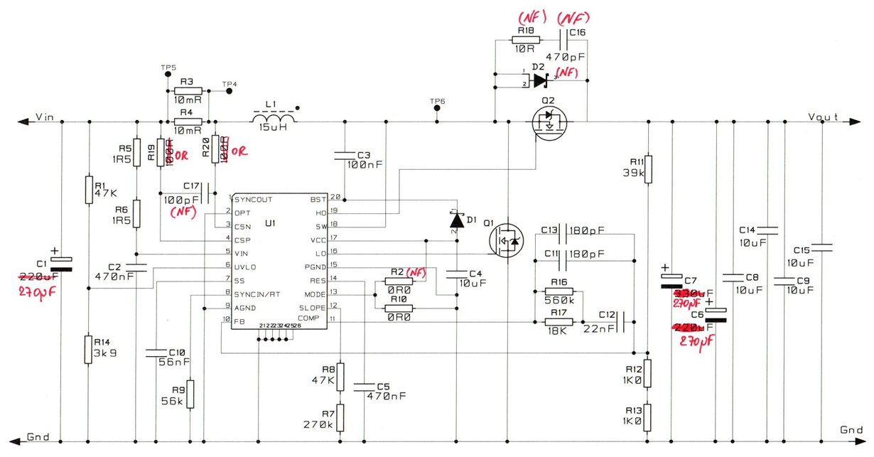
see below schematic, the layout has been made based on the LM5122EVM-1PH
Q1 CSD18503Q5, Q2 CSD18509Q5BT

What I have noticed

1) the problem seems to happen when the high side FET starts being driven.

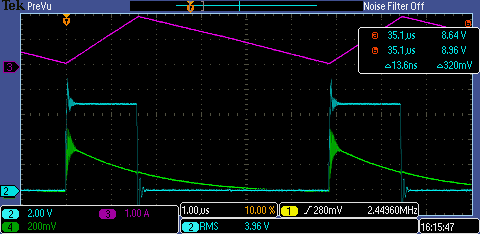
2) pulses are generated on the RES PIN when the low side FET is turned ON

Below are scopes captures made with a ~700mA load (C5 replaced by a 27k on RES PIN to see when the limit operate)

CH2 gate of Q1,CH3 current in L1, CH4 RES PIN


  • Schematic and scope captures mentioned in the 1st post.

  • Hi Gilles,

    Thank you for considering the LM5122.  If you schematic is accurate, then the RES should not source current.  Instead, there is a 5uA sink into the RES pin.  However, your waveform shows a sourcing current, implying the RES capacitor ground may be pulled lower than the AGND pin.  This implies a ground issue, that you may not separate PGND and AGND on your circuit board. 

    PGND is for power signals, and AGND for control signals.  They should be separated, only connected at a single point to prevent the noisy PGND to affect the control signal.  Refer to our EVM layout and follow the example to separate the AGND and PGND.

    Thanks,

    Youhao Xi, Applications Engineering

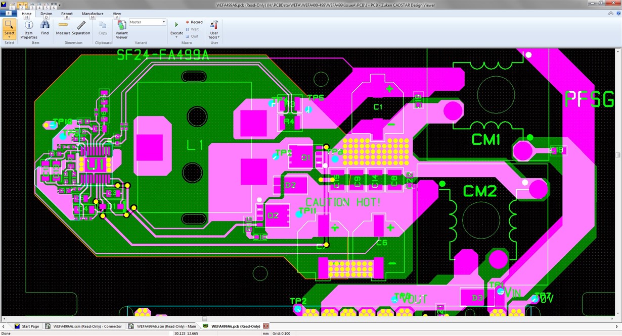
  • Thanks for your reply.  Could you help identifying the problems in the below layout.

  • Is this a two-layer  board?    When you capture the waveforms, where do you place the ground lead of each probe?

  • That is a 2 layers board

    CH3 is a current probe, so no connection to ground

    CH2 short wires (~1cm) soldered between gate and source of Q1 (PGND)

    CH4 short wires (~1cm) soldered across C5 (AGND)

    You put me on the right track in your 1st reply, mentioning PGND and AGND should be separated. When comparing our layout and the EVM layout, I realized the ground of the Vcc capacitor C4 was connected to AGND. I moved a bit C4 and drilled a hole to connect it to PGND using a via and now it seems I don't have hiccup overload issue. I did the change on 2 boards and was able to load them to 8A.

  • Thank you Gilles for the confirmation.

    Actually your layout looks basically good.  If you want further improvements, please consider to put the SW trace to the FET be closer to the HO trace over the entire length from the IC to the FET.   Also consider to swap D2 and Q2 position, because Q2 conducts most of the current, and it should be closer to Q1. 

    The two probes grounding pins, introducing additional connection between the AGND and PGND, simply defeating your effort of making single point connection.  To monitor sensitive signals, just use one ground pin of the probe for the signal that you cares most, and do not use ground probe for other signals which are just monitored as references.

    Thanks,

    Youhao

  • Hi Youhao,

    I will follow your recommendations, I think I am going to remove D2 and move Q2 closer to Q1 also improving the layout of the gate drive.

    I performed different load tests on my prototype and functionally everything seems all right. The only think wrong I noticed is a 60MHz oscillation when driving the bottom side switch (see attached scope  capture performed with 2.5A load CH1: switching node, CH2: bottom switch gate, CH4: output probes are 300MHz probes using short wires all connected to PGND). I tried the snubber on the high side switch, but I was not able to change the frequency of the oscillation.

    Could you tell me which area to investigate to dampen this 60MHz ringing? 

    Thanks.

  • On your circuit you can try the snubber (C16, R18).  If you have a gate  resistor, you may use it, too,  but currently your circuit does not have one. 

  • Thanks for you help.

    I managed to dampen the ringing on the high side switch using 1nF 4R7 for C16, R18 but I noticed I also had a ringing on the low side switch for load above 4A. After some experiment I also added a 1nF 4R7 snubber on the low side switch.

    Am I right adding a snubber on the bottom switch ?

    Is 1nF 4R7 not too aggressive for a snubber ?

    The scope capture shows the switching node without C16, R18 (R2) and with 1nF 4R7

  • Hi Gilles,

    If the two FETs are close, then only one snubber should be adequate. The two snubbers have the same effect:  damping out the ringing (ac signal) between SW and a dc potential.  For ac signal, GND and VOUT is the same.

    1nF sounds aggressive:  0.5 x C x V^2 x Fsw will be the snubber losses.  See if you can reduce C to 330pF of smaller, but increase R by the same factor? 

    Thanks,

    Youhao

  • Is the issue resolved?  Let me close it here but you can re-open it by add a new post.


    Thanks,

    Youhao

  • Hi Youhao,

    Yes the issue is resolved thanks for your help.

    Gilles