Hello
I have some questions, Please help to solve,thanks
1.How much negative voltage/min volatge does SW pin could understand ?

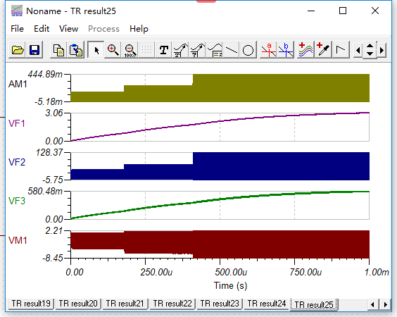
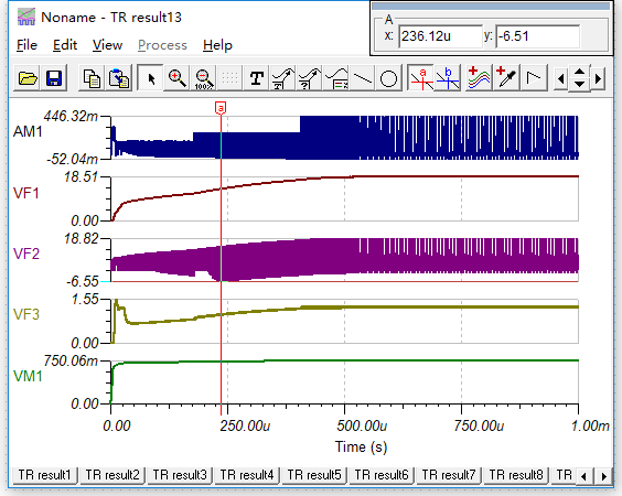
2. I use TINA simulate the Figure17 SCH in datasheet, below is the TINA-SCH and waveform, I find the SW pin will be drop to -6.55V , I don’t know how that happened, do you have some comments here ? and could -6.55V possibly damage the device ?

3.Output capacitor C2 could palce at the behind of PNP ? I place it behind of PNP, and all waveform have some abnormal. especial for SW,max 133V,min -14V. Could you explain it ?
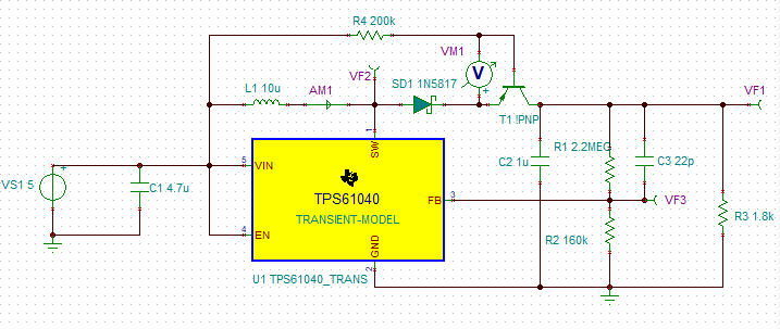

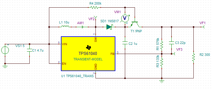
4.Actually my customer SCH is show below, Vin 5V, Vout 6.5V. load current maybe need dozens of mA, I place 300ohm, simiulate 20mA load. And I find SW Pin also have -6.6V, is there any risk?