This thread has been locked.

If you have a related question, please click the "Ask a related question" button in the top right corner. The newly created question will be automatically linked to this question.

LM3409EVAL: Issues with obtaining current waveforms as shown in Demo Board Users Guide

Part Number: LM3409EVAL
Other Parts Discussed in Thread: LM3409

I'm trying to use the 3409 chip on its DEMO board, using EN for PWM. I am trying to drive single high-power LEDs. For instance 6A at 6V. I have beefed up the PMOS FET as well as the schottky diode and inductor.

I am trying to run the power supply loop at 1 MHz and the PWM at 20kHz.

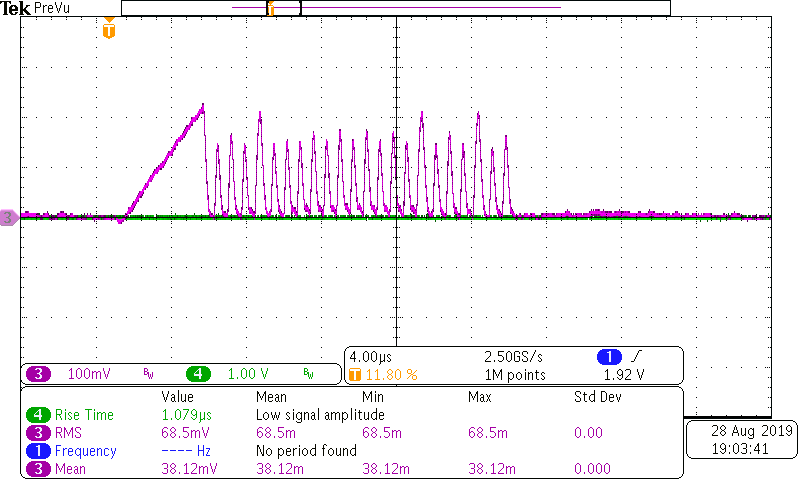
Picture below is differential voltage across my sense resistor (0.033 ohm) which makes the scaling about 3A / box.

My problems seems that I cannot lower my delta current to a value like 500 mA. Note that my pp current is 3A. I cannot get a current picture like the one on the  Users Guide Figure 5 (not the 3409HV users guide)

In figure 5 the current steps up from zero to about 1A and then the pp current centers around a 'DC' level of a with a pp value of about 0.5 Amps.

I would appreciate any insight you might have regarding this problem.

I need to have lower pp current to get a close-to linear output current when varying my PWM. 

Thanks, Rich


  • Rich,

    What is the total gate charge (Qg) of the new PFET you are using.  If it is above 30nC (which is likely due to your higher current capability), the datasheet explains that you need to change the connection of your VCC capacitor (new connection would be from CSN pin to VCC pin).  This will  prevent the very large spike of current from the gate drive circuit from false tripping the sense comparator and should stabilize the peak detect value.  That's the most likely reason for the abnormal peak detection.

    Regarding peak to peak ripple, you simply need to use a different inductor if you want to reduce that.  For example, doubling inductance will half the peak to peak ripple at a given switching frequency.

    -JP

  • JP,

    Thank you for your insights. My PFET does indeed have a Qg of 36 to 45 nC (SPD30P06PGB).  Could you please point me to the the part of the data sheet that addresses this issue?  So I will take the capacitor presently connected from Vin to Vcc (1 uF) and connect it from Vcc to the CSN pin.

    Re pp ripple: there is an equation in section 8.3.4 of the LM3409 data sheet that states the minimum pp current needs to be no smaller than 24 mV/Rsns.

    Since the maximum LED current is ~240mV/Rsns that reads to me that the ripple can never be smaller than 10% of the LED current. e.g. if you are delivering 5A of current to the diode, the smallest you can make the ripple would be 500mA pp. Is that correct? Or could I make the ripple 100 mApp which would give me a smoother current waveform?

    Thanks,

    Rich

  • Rich,

    Section 9.1.8 in the datasheet describes the Qg>30nC situation.

    Regarding the peak to peak inductor current ripple, yes there is a minimum ripple requirement and yes, it equates to 10%pp minimum as you calculated.  In the case of the evaluation module (which I think you are referring to the non-HV version AN-1954 given you called out Figure 5 and the 1A design), it is designed for 1A with the RSNS=200mohm.  Therefore the ripple can be a small as 100mA in that case.  With the chosen inductor of 22uH and Vin=24V and Vout=15V, you can achieve this performance in figure 5.

    With Vout = 6V, and whatever VIN you are using, and the 5A requirement, you will not be able to match that performance.  It's possible you can add output capacitance to attenuate the LED current peak to peak ripple further, however that will create longer rise and fall times during PWM dimming.

    -JP

  • JP --- additional questions if I may.....

    You say:

    With Vout = 6V, and whatever VIN you are using, and the 5A requirement, you will not be able to match that performance  in Figure 5 of the non-HV Demo board.

    Could you tell me what would be the limiting factors in trying to run up to 5A and hope to get a waveform that looks like Figure 5 as opposed to the scope trace I included at the top of this thread?  I've done you mod of moving the bypass capacitor from Vin and moving it to CSN. That cleaned up the current trace but it still swings from zero to 5A (at my switching frequency of 1 MHz) when EN is enabled. 

    Follow on question: If the best I can get is a current waveform the swings between zero and say, 5A, is that going to be stressing some part of the circuit that I'm missing?  I know I will need to heatsink the PMOS FET and the freewheeling Schottky diode.  This circuit may perform to my needs but I don't want to settle on something that is making the parts really unhappy from the get-go.

    Would this conversation work better by phone? I'd be happy to call.

    Rich

  • Rich,

    Please verify exactly which board you are using (you can reference AN-1953 or AN-1954), exactly which components were replaced and with what.  And please confirm your test setup.  Power supply voltage at input, current limit setting on power supply, and measured input and output voltage at the terminals of the evaluation board.  Then I will run the numbers and tell you what you can expect.

    -JP

  • OK, I can do that.

    I'm working with AN-1954, the NON-HV board.

    I'm referencing the schematic Figure 2 and the BOM (section 4)

    VIN is either +12V (preferred) or +24V from a supply that will source 15A (I have no current limiting set on the power supply)

    I'm adjusting R5 pot to obtain an output current that swings between zero and +3A with a switch freq of 1 MHz.  

    The measured voltage on LED+ when driving +3A is measured as 3V DC on a DVM

    The measured voltage on LED- is zero.

    I am doing my PWM with an external pulse generator. The PWM is being done by connecting a schottky diode from the waveform generator to the UVLO pin (removed R2 and R3) That seems to make the ON time of the initial ramp to be faster.  PWM freq is 30 kHz.

    The EN pin is tied directly to VIN with jumper J1.

    These are the BOM changes compared to App Note BOM

    1. C4, 1 uf connected between Vcc and CSN
    2. Q1 PMOS 60V, 30A, p/n SPD30P60PGBTMA1
    3. D1 SCHOTTKY 45V, 15A, p/n SK1545
    4. L1 6.8uH 13A, 8.98 mOhm p/n 7443320680
    5. R1 2K00
    6. R2 removed
    7. R3 removed
    8. R4 0.033 Ohm

    Look forward to your response,

    Rich

  • JP:

    I've attempted to attach a PDF of the data sheet for the LED I'm driving. If it is not attached, this is a link to it.

    https://www.mouser.com/ProductDetail/Luminus-Devices/SSR-90-R-R11-HG100?qs=AafiUGZxyHaQrCvqJn30qg%3D%3D

  • Rich,

    Looking at the calculations for this, what you would ideally see given your components is 220mA of peak to peak ripple at these operating points, therefore this is definitely not regulating properly.  Also, looking at the waveform again, the inductor slopes look totally wrong for the voltages.  Your Vin is much higher than your Vout, so the initial slew rate makes sense, however each one following is far too steep (rising slope is (Vin-Vout)/L.)  This is also a relatively high nominal current which this EVM is not designed for and your inductor may be saturating due to temperature rise (which could be why the slew rates look so steep).  You really should make your own board with proper thermal considerations.

    Also, Given your component values I calculate more like 1.7MHz which gives you a period of 588ns.   If your VIN is 12V and your Vout is 3V, then your ideal duty cyle is 25% which gives you a 147ns on time (very close to our minimum on-time).  At 24V Vin, you definitely won't operate at 1.7MHz as the duty cyle is 12.5% and the on time is 70ns.  So, this is a problem also and would create a ratcheting effect increasing the effective pp ripple.

    In general, that is far too high of a switching frequency for these currents.  The IC is likely extremely hot and could be outside of its operating range.  Your switching losses wil be huge and this is very impractical to implement at a system level.  I would drop the switching frequency to sub 500kHz by using a 3 or 4 times bigger off time resistor and increase my inductor to compensate for the desired switching ripple.  Much better design in my opinion.

    -JP

  • James:

    Thank you for your in-depth response.  I've been trying to answer the big-picture question which is: "Is this the right approach for driving 6A LEDs"?  I'm getting the feeling is kinda not. It was a part suggested to me because it has the features of PWM dimming and the ability to set the maximum current via the iADJ pin

    Could you point me to a diode driver that may be better suited for my application?

    Rich

  • JP I hope I can ask you a few more questions about this. I have two AN-1954 Demo boards. The first one I put in some of my own components. That is the circuit I've been discussing to this point. But since I've made my own component changes its been harder for you to help.

    So, I took my second demo board and did not change any of the factory components. With the hope that  if I configure it to No PWM, EN=Vin (done with jumper J1) and Vin = 24V. Driving a single power LED, I would get waveforms similar to Figure 8 of the AN-1954 guide.

     I am running wires from the board to the LED that are about 3 inches long (16 ga)

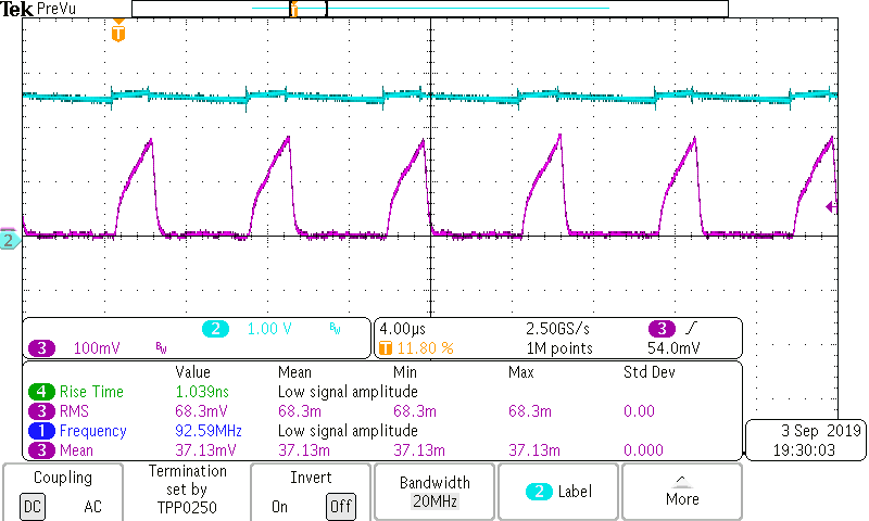
    The waveforms are shown above, you will note they don't look like Figure 8. The lower trace is differential voltage across R4 (0.2 ohm)  That makes the Vert sensitivity to be 500 mA/box

    The upper trace is the voltage across the LED at 1V/box.

    In one of your previous responses you mentioned that the circuit was not regulating. Does my data show the same thing?   Since I'm using a factory stock board can you give me any guidance towards getting it working correctly?

    As always, thank you for your time.

    Rich

  • JP. Please disregard all of  the measurements shown towards the bottom of the screen. These were holdovers from different tests.

    Rich

  • Rich,

    Your operating points are not the same as the figures show.  As I mentioned before, this is a hysteretic converter, so the frequency and operation depend on the voltages at the input and output.  Looking at your waveform, the output voltage is below 3V and I don't know which input you are using (12V or 24V), but that matters.  Figure 8 uses input of 24V and output of 15V.  Therefore your frequency will be lower given you have much lower Vout.  When your frequency decreases far enough you enter discontinuous conduction mode (DCM) where the inductor current slews down to zero every cycle.  Your waveform shows that you are in deep DCM.  In DCM, you will not regulate properly with this type of converter as it is measuring peak current and expecting CCM operation.

    You really need to run the calculations for your operating points and determine the correct design from there.  If you want to duplicate the EVM, then apply VIN=24V (ensure your supply is not limited and measure VIN at the board to verify operation) and VOUT=15V.  Then Figures 7 and 8 should show you nominal operation with no PWM at maximum IADJ (R5 fully clockwise rotated) and  minimum IADJ (R5 fully counter-clockwise rotated).

    -JP

  • JP:  Good insight.  I will make a load across VOUT that will generate 15V. 

    Question: I'm a little short on power LEDs to build a load.  Can I simply make a resistive load (of about 15ohm) or is the circuit expecting the dynamic characteristics of an LED load?

    Rich

  • Rich,

    Yes, you should get a similar waveform.  Obviously your voltage varies much more across a resistor than a diode, but for observing a single operating point such as the ones in Figs 7 and 8, a power resistor should work fine.  Pay attention to the power rating as you have to dissipate 15W at 1A!

    -JP

  • Rich,

    I apologize for the delay in response. Is this something you still needed help on or has it been resolved?

    Regards

    Sumeet

  • Thank you it has been resolved for now.

  • Thanks for confirming. I will close the thread.

    Regards

    Sumeet