This thread has been locked.

If you have a related question, please click the "Ask a related question" button in the top right corner. The newly created question will be automatically linked to this question.

LM3401: Same Design and BOM not working after 3 year gap

Part Number: LM3401

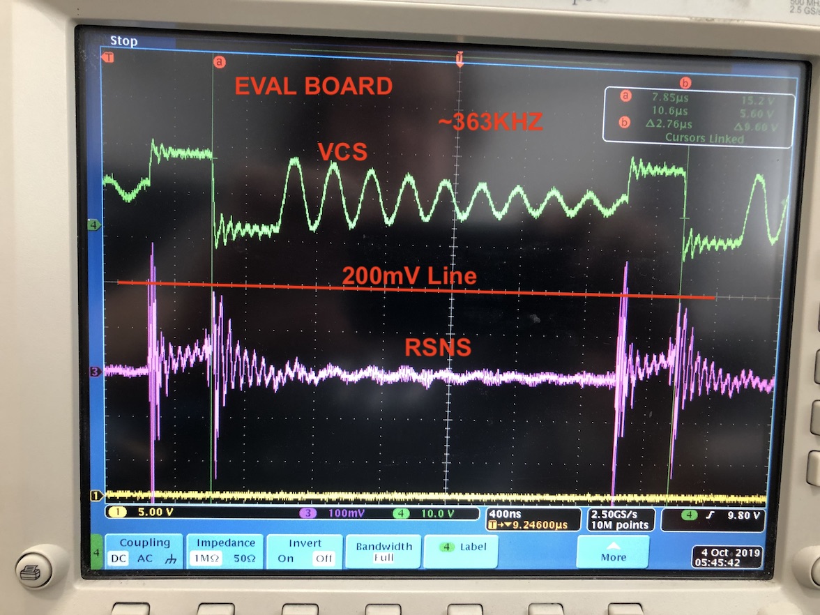
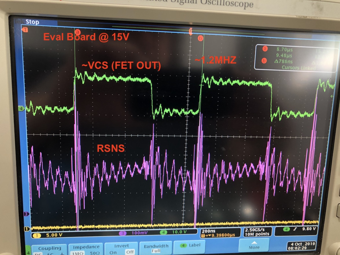
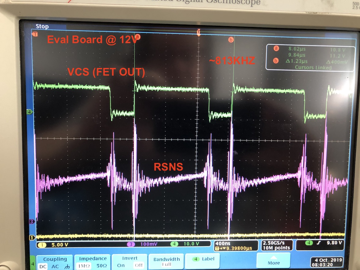
We have a design with the LM3401 with 3 LED's in series.

A 9V forward Voltage. 24V Input.

The first build of this was done in Feb 2017 in china.

The second build was done this year in the USA.

This is a MCPCB.

Both builds used the same GERBER's and BOM.

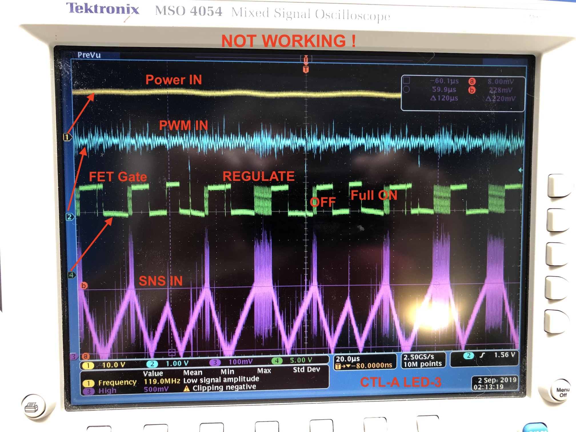
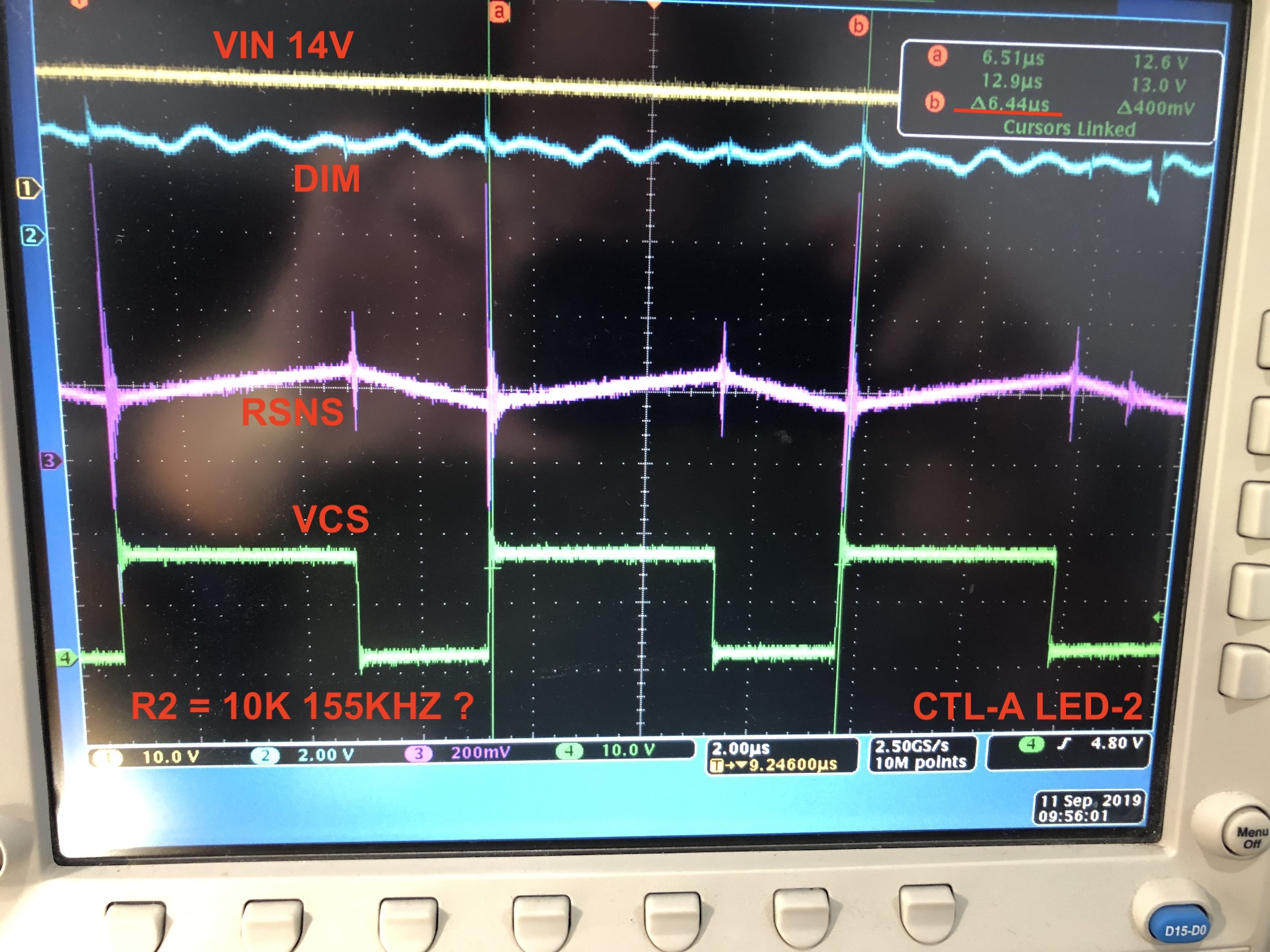
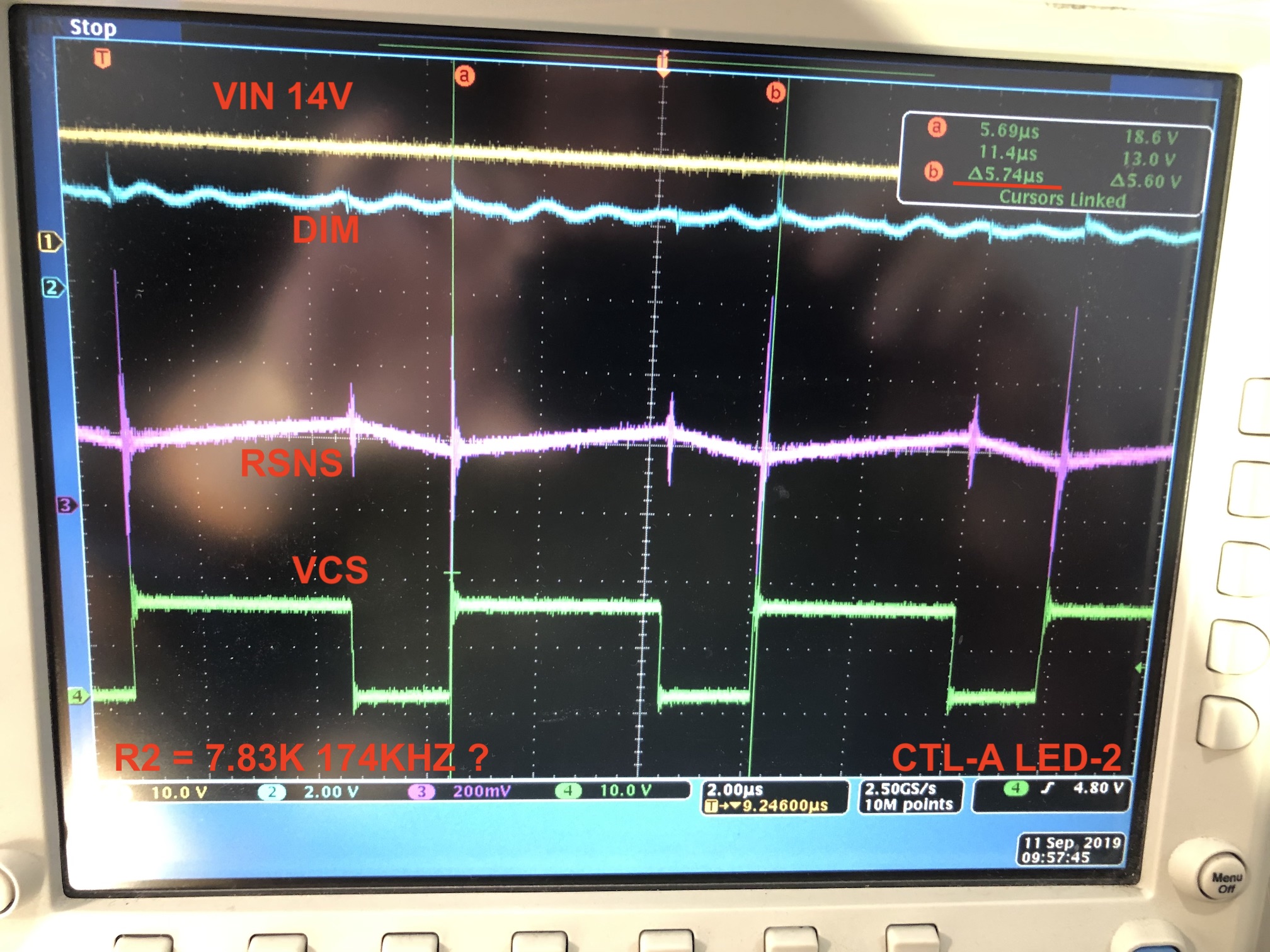
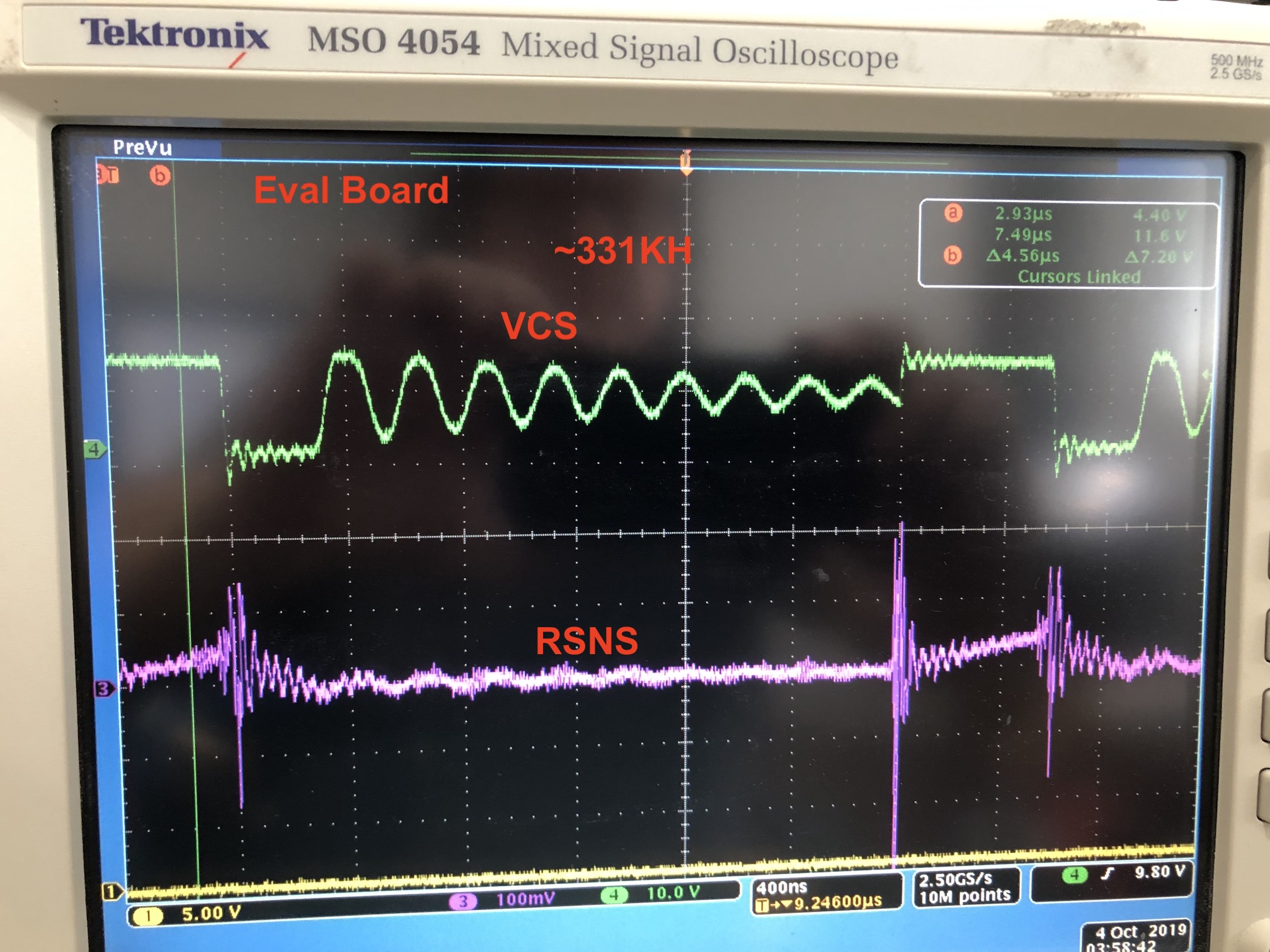
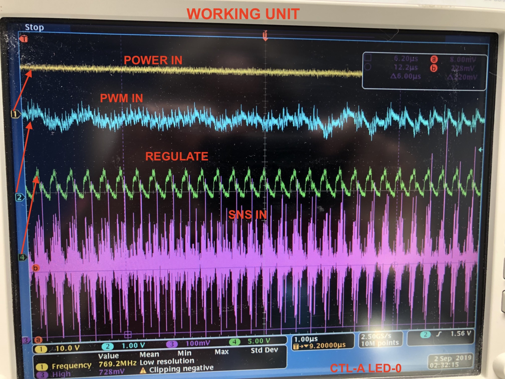
I see erratic behavior on the Gate drive that I do not know where it is coming from.

Working Unit:

Not Working Unit:

  • John,

    Please explain your labeling here.  These waveforms do not make sense in either case (working or not working).

    I need to know exactly what PINK, GREEN, BLUE, and YELLOW are in the circuit (voltage or current, and what exact IC pin you are measuring).

    Right now, if I read labels on the oscilloscope waveform, even the "working" PCB is not functioning properly at all.  For instance, if the blue waveform is the voltage at the DIM pin of the LM3401, then it should either be a DC voltage or a PWM waveform at the dimming frequency.  The blue waveform is extremely noisy and not DC or PWM'd.  That can cause erratic behavior.

    In any case, I can't start to troubleshoot this until I am sure what each waveform is.  Thanks.

    -JP

  • Yellow:  Power In.   Pin 7

    Blue:  PWM  Pin 2.   It is a little noisy, but I thing that is scope GND issues.  it is high.

    GREEN:  Gate Drive of Fet,  HG,  PIN 6.

    Pink:  Current Sense resistor or PIN 3  (SNS).

    The same power source, PWM IN at the same setting are used on both boards.

    Each using the same BOM and Gerber. 

    I think the controller may be damaged and will try replacing later today. 

    I have used a micro-ohm meter to verify that all resistances from GND to  pins 3, 5, 4 are the same on both boards.

  • John,

    Thanks for confirming.  And, I have bad news for you.  The original circuit is most certainly not operating correctly.

    The gate drive (green waveform) looks awful.  It should be a square wave.  That's probably because it is switching at close to 3MHz at the operating point you are showing, and the gate charge of the external PFET is probably too large.  Frankly speaking, I am surprised this circuit isn't melting off the board.  Most likely you are violating the junction temperature maximum of the IC at this switching speed in which case, who knows what's happening.  I am certain that the PFET is not being fully enhanced (turned on) during the switching period which will lead to very high cross conduction losses in the PFET.

    And, the SNS voltage (pink waveform) is completely noise, so the 3MHz is likely a function of the sense circuit false tripping.

    In general, the capacitive coupling on MCPCBs is extremely high and it is very difficult to make a switcher like this function properly without noise problems.  Any bit of difference in the dielectric of the MCPCB stackup (material type, thickness, etc) will change the effective capacitance and associated noise signature so that could be what's different from one revision to another.

    Your circuit should have waveforms like those shown in Fig 15 of the datasheet.  Those are actual waveforms from a designed converter.  There is minimal noise and you see a nice triangular waveform for VSNS and a nice square waveform for VCS (and HG will look like VCS only inverted and level shifted up to VIN.)

    Finally, have  you run calculations on your expected operating points?  This is a hysteretic converter, so your switching frequency varies with input and output voltage.  You can calculate the expected switching frequency from the equation on P.9 of the datasheet.  If it is too high, then you can either increase the hysteresis (ripple) or increase the inductance to reduce the frequency (or change both).

    Either way, there is way too much noise on this application to use a hysteretic converter.  That must be attenuated to properly operate.

    -JP

  • I have check the components and measured from my GND connection to R1 and R2.  That all checked out.

    So here are the calculation I just backed into as I was not the designer of this:

    R1 = .110 ohm

    R2 = 3.48K

    R3 = 88.7K

    Current:    I = 200mV / Rsns(R1)  =  .200 / .110   =  1.818A

    SNShys:  R2 = (SNShys *5)/ 20uA   =  R2 * 20uA = SNShyx * 5   = (R2 * 20uA)/5  =   (3480 * .00002)/5  =  .0139mV  ~.014mV

    Vin = 13.7 V

    VAnode = 9.46   (max LED forward for 3 LED’s)

    L = 33uH  @ 5.5A

    FET Delay =  19ns

    FED Ron max = 19mOhm

    LM Delay = 46ns

    Rsns = .110 ohm


    <image001.png>

    D = Duty Cycle  = .96


    Fsw = .96 / (  (  (2*.0139*.000033) /    (.110 *(13.7-9.46)  )  )+(2*(.000000046+.000000019)))  =  457,800 HZ

    So all this looks good so far.

    Very tight SNShys.


    R3 does look to be way to high.

    Based on:

    R3 = ILIM_PK * RDS(on) / 4uA  =  (2.18 * .019) / .000004  =  10.363K   not the 88.7K


    That is the only issue I can find with the design values.

    My next step is to replace R3 with 10K and try new IC (LM part).

  • John,

    1. 1.8A switcher design on and MCPCB!  No wonder you have noise problems on the original board.  And with 14mV hysteresis its very likely false triggering hence why I don't see proper regulation.

    2. Your duty cycle is not 96% at these operating points.  The ideal equation is simply Vout/Vin.  Even with losses that should only be a little bit higher.  The equation in the datasheet adds the forward voltage of the switching diode to Vout (roughly 500mV you can assume at high temperature which you definitely will have) which gives you D ~ 10V/13.7V = 73%. 

    3. R3 is the current limit.  If the resistance value is 8 times higher than you are calculating now, then you are likely running into it before the actual peak sense of the hysteretic comparison on R1.  You are right, it should be a much lower value. 

    So, as I said, I don't think this design ever worked correctly given all these details.

    -JP

  • I am back after doing a lot of leaning on the part, but still am a little confused.
    First, I see that there is a Calculator available, but I can not find out how to get it:  LM3401DESIGN-CALC:  LM3401 Component Calculator
    I have attached an xlsx of my calculation.
    The calculations are close for 10K and 7.83K, but the 3.48K will not work.

    The thing that is missing is why the FET/Inductor is not able to regulate with a very small HYS?
    Is there an equation that can be used with FET Delay and inductor that can calculate min HYS?

    I think that the Inductor (WE 7443551331 is not working as expected.
    The ramp up time is twice the discharge in the images I have added.

    The new images show that 10K works, but is not fast enough for the application.  But the FET / Inductor is not recovering fast enough to go faster.  I would like to get to about 500KHZ at 1.8-2A.
    Event though the 3.48K should be a good value for the HYS, its not clear the FET/Inductor can work fast enough.

    The other thing I found is that the demo board uses 100 ohm and .1uf on the VIN, I would expect this is noise reduction. I was thinking of adding this to the VIN of LM3401 and DIM lines.
    Also on the DIM line, keep any off signal at a minimum of 500ns or longer so there are no fast off/on on this pin.

    I am very course about the Design-CALC to see what was done in it.

    We use the light source for clients with very high speed photography at about 1/10,000 sec shutter speed and/or frame rate.

    The big question at this time, can I get faster than 300KHZ regulation at current about 1.8A and what would it take?

    Thanks.

    Versa.xlsx

  • All the wave forms in the data sheet show the VSNS (RSNS) rising faster than it decades.  What would cause mine to do the opposite?

    Is that the value of R3 which is set at 88.7K?

  • John,

    You should definitely read up on switching regulators in general.  Your last question relates to the basic operating principles of a buck converter.  The rising slope of the inductor current on a buck converter is defined by the equation (Vin-Vout)/L and the falling slope is defined by the the euqation (-Vout)/L.  Therefore the difference in any comparison of two different inductor current waveforms can be determined by comparing Vin, Vout, and L.  In your case, if your rising edge is fast and your falling edge is slow, then your duty cycle is low...meaning that Vout is much smaller than Vin.

    Regarding your specific questions on your design, the practical nature of implementing a hysteretic switching converter can limit hysteresis achievable.  The delays in the comparator path as well as the speed of the switching itself will limit the acheivable hysteresis.  However, your PCB layout and stackup is equally as important.  As we have discussed already, your system is extremely noisy.  Therefore, small hysteresis will definitely not work.  That noise will false trigger the comparators and completely affect regulation accuracy. 

    I am fairly certain your implementation is limiting what you can acheive.  I think it would help if you purchase an EVM and use it to tune your desired regulation point.  Then compare it's performance to your PCB behavior and determine where the problem is in your circuit.  You most certainly can make a design that operates at 500kHz and 1.8A at the nominal operating point, but remember...when you change Vin or Vout the frequency will change.

    Also, remember that with a hysteretic converter, you can leave the hysteresis at the larger value, and increase frequency by decreasing your inductor value.  It seems like this may be a better approach with your PCB given the noise problems when you minimize the hysteresis.  This shouldn't affect your design too much as the smaller inductor value will have lower DCR (better efficiency) and will be in the same package or smaller.

    -JP

  • Thanks for this input.

    I have ordered the Eval Board and a number of inductors for mine.

    I have a version of the design that is two boards.  The LED's are on the MCPCB and I have a second which is a 2 layer board with the bottom being mostly GND and VIN. There are openings in the second for the LED's to shine through.  I will start working with this and see how it dose.  It looks like I need a much smaller inductor.

    Will up date in about a week.  Take some time to get every thing and document the setups.

  • In continuing with my research and education on this part I found the Webench for this and it has shown that my inductor is to high.
    The 33uH should be lower than 10uH.

    Doing a 2A drive of 3 LED's is no problem.  But when I try to get to 4A I get a junction temp issue.
    Not sure why as the FET and inductor should be fine.  I do run the Webench at 50C with custom LED.
    Forward Voltage:    2.85 Typ,   3.15 Max
    LED I :    3A Max

    The 4A configuration is 3 in Series  6 Group  at  .666A.

    It would be nice for the Webench to show the VRsns in the simulation.  Is there a way to add that?

  • John,

    Please share your WEBENCH model.

    I can't change the WEBENCH interface on a 15 year old device, but I can look at your model and perhaps provide insight.  I agree that the current through the LEDs shouldn't change the temperature of our device, however the voltage relationship of input and output will change the frequency which will definitely affect our junction temperature.  Therefore, the 4A design is likely a higher switching frequency. I keep coming back to the same point here.  Frequency is key.  High switching frequencies are very difficult to accomodate in switching converters.

    -JP

  • I think you are right. We are exceeding the infrequence of the part.
    My 2A 3 LED design is running at about 1.4 or 1.3 MHZ.  If I am going to double that I should be way over the 1.5MHZ Max.
    https://webench.ti.com/appinfo/webench/scripts/SDP.cgi?ID=6F84E8C190EA2C9A

    So I can use the same 2A design and just double the circuits.  I think I have the room for that.

    https://webench.ti.com/appinfo/webench/scripts/SDP.cgi?ID=C9A17F34273C00FB

  • John,

    Do you need further support on this? If not, I will close the thread.

    Thanks

    Sumeet

  • Yes I do....
    This is the pass I just finished.

    I just took the Eval Board and change the inductor, R1, R2, R3, CIN and COUT and it does not work anything like the Webench sim.
    I have the parts off my LED board(MCPCB) and wired to the Eval.  The power from the controller is 12VDC at 100% on.

    The good news here is that I am not seeing the runaway as before.

    I still have to make a run at the higher voltage.

    R1 = .100 ohm
    R2 = 6.85K
    R3 = 7.15K
    L1 = 5.8 uh

    CIN = 6.8uF
    COUT = 10uF

    Even though the switching time is over 300KHZ,  there is still a lot of dead time on the current going though the LED's.

    The RSNS input is not getting to 200mV as it should either.  So why is the FET turning off early?

    Just did a run at 15V and the speed only increased to ~363KHZ.

    Still not seeing it SNS get to 200mV.   Will try changing the FET.

  • This equation may not correct in webench from what I can tell.
    R3 =  (4A x .100 ohm ) / 4uA   = 100K  not 7.15k
    Both voltages are working now.  I just need to knockdown the noise on RSNS.
  • Hello John,

    Are your circuits working correct now?  I will be trying to help if you have any issues.  I have a mathcad spreadsheet started to calculate your circuit operation.

    Best Regards,

  • Yes they are.  Yesterday I was able to get the target board working with following values:

    L1 = 15uH @ 4.4 A
    R1 = .110 ohm
    R2 = 6.18K
    R3 = 130K  This was the biggest error in Webench for the part.