This thread has been locked.

If you have a related question, please click the "Ask a related question" button in the top right corner. The newly created question will be automatically linked to this question.

part failure

Part Number: LMZ31707
Other Parts Discussed in Thread: LMZ31704

Hi,

We have recently encounters 3 cases of catastrophic failure with the LMZ31707 in our design. The LMZ31707 was design to power the 3.3V rail for 4 QSFP pluggable modules in the system. The total max load current for all modules was designed for 6A, as such, there is a 1A buffer in the design.

Case (1) - The unit under test was loaded with four QSFP modules, the total load current is about 4.8A, running in the envirnoment chamber at 55 degree C with 90% humidity for 24 hours before the LMZ31707 fails. The VOUT was found to be shorted to PGND.

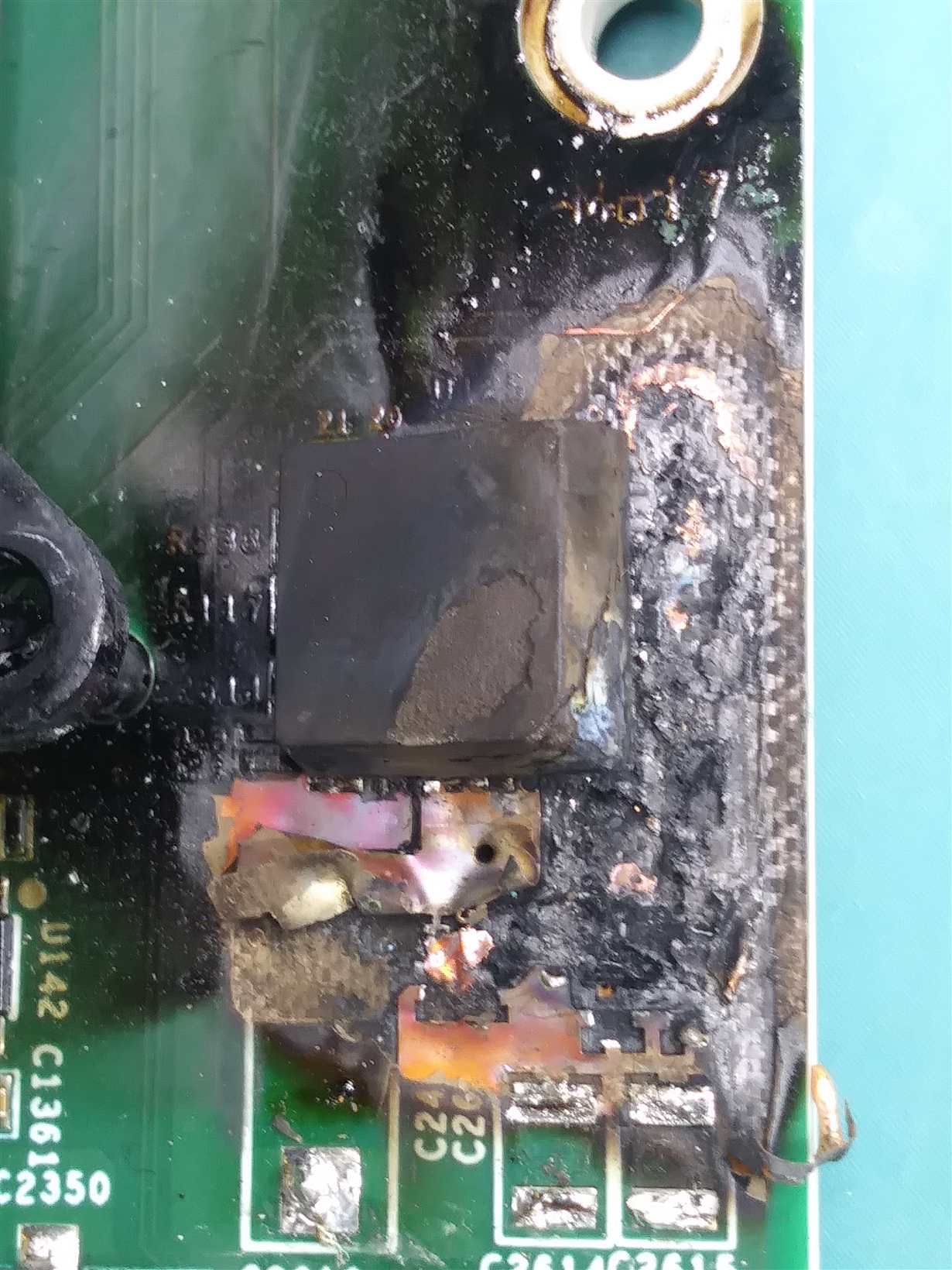
Case (2) - Same test environment as case (1) except that only 2 QSFP modules were installed, the total load current is about 2.4A. The uut was left to run overnight, it was found burnt the next day. The LMZ31707 and the input/ouput  capacitors were badly charred.

Case (3) - This was a customer returned unit, operating probably in a room temperature environment. The LMZ31707 and the input/ouput capacitors were badly charred.

We did 2 experiments to try and re-produce the failure without any conclusion.

Ex (1) - at room temp, without any QSFP load, shorted the VOUT to GROUND and power on the system. The case temp on the part rise to around 58C and then it start to drop and stablized at around 52C. I am assuming that the Thermal Shutdown function kicks in. The part function normally after again the short was removed.

Ex (2) - in the environment chamber at 55 degree C and 90% humidity. Connects VOUT to a electronic load, drawing 7A, the case temperature measured around 73C. After 2 hours, the LMZ did not shut down and UUT is still working. The uut is left to run overnight until tomorrow.

It looks like this might be related to thermal rather than the Over Current issue.

Can you take a look and see what might be the root cause of this failure?   

I have attached both the schematic and the PCB layout.

schematic-pcb.zip

  • Hello Tan, 

    Thank you for providing the schematic and layout. 

    The team will review and provide comments. 

    Cheers, 
    Denislav 

  • Hi Denislav,

    Below is a picture of the burned part, looks like the fire starts at around pin 1,2,3 area.

    Thanks,

    SB

  • Hi Tan,

    Looking at your schematic and layout, it does not appear as though AGND is separate from PGND as the LMZ31707 datasheet recommends (p.6 and p.26). There may also be insufficient connection/stitching to PGND at pins 20 and 21. The layout could also benefit from input cap placed closer to pin 11 and 12 PVIN pins as shown in the datasheet p.26.

    What are the voltage ratings of your input and output capacitors?  

    (Though it may not be an issue, I also noticed that you have 44uF ceramic cap, while the datasheet recommends 47uF minimum ceramic on p.12)

    Can you probe the input and output voltages to see if they are stable?

    Is your Ex 2 board still running fine?

  • Hi Kris,

    The AGND and PGND are not connected on the top layer, they are tied together in the inner ground layer. I agreed the layout could be improved further.

    The input capacitors are rated 16V for the 100uF and 0.1uF, and 25V for the 22uF.
    The output capacitors are rated 4V for the 470uf and 6.3V for the 22uF.

    The input and output voltages are stable.

    The Ex 2 board, the output is still fine after the overnight test.
     
    In normal operation, is there any effect on the output signal integrity between cycle-by-cycle and hiccup mode?

    Do you have any clue as to what might have causes the part to burn?

    How can I send the fail part from case(1) back to TI for failure analysis?

    Thanks,
    SB
     

  • SB,

    TAN SB said:

    In normal operation, is there any effect on the output signal integrity between cycle-by-cycle and hiccup mode? 

    Can you please clarify what you mean by effect on output signal integrity in cycle-by-cycle versus hiccup mode? These are two different responses to overcurrent conditions as described in Section 9.19 and both result in changes to output voltage behavior.

    TAN SB said:

    Do you have any clue as to what might have causes the part to burn?

    I think you have done some good experiments Ex 1 and 2 that have ruled out anything obvious.
    You probed input and output with an oscilloscope, right? Can you also probe the PH switch node on a working board? Perhaps there is excessive ringing at this node leading to voltage stresses beyond the abs max rating. Improvements to layout, especially the capacitor placement, could help improve any ringing you observe.
    TAN SB said:

    How can I send the fail part from case(1) back to TI for failure analysis? 

  • Hi Kris,

    I might have miss the following response in the earlier reply:

    What I meant regarding the OCP mode is, is there any effect on the output voltage ripple between cycle-by-cycle and hiccup ?

    Yes, I probed both input and output with the oscilloscope.

    I have attached the signals captured for the input, output and PH node.

    There are 5 captures for the PH node, with no QSFP module installed and with different number of QSFP modules installed. There is no difference for both input and output regardless of the load condition.

    What minimum gap size between the PGND and PVIN and VOUT plane on both internal and external layer of the PCB would you recommend?

    Thanks,

    SB

  • SB,

    The output voltage behavior is very different between hiccup and cycle-and-cycle modes as shown in datasheet Figures 30 and 32, so I am not sure what you are trying to compare with regards to voltage ripple.

    I looked the EVM layout files, and the gap between the copper pours is about 10mils.

    Regards,
    Kris

  • Hi Kris,

    Did you get a chance to look at those signals on the PH node I sent earlier?  Any suggestion on the placement of the capacitors and the layout for further improvement?

    Thanks,

    SB

  • Hi Kris,

    This afternoon we encounter another similar part, LMZ37104, used in a different location on the board popped and burned in a similar pattern, fire originate around pin 1, 2, 3 and the input capacitors.

    Do you think the input ripple current might be the cause of the fire? These are the input capacitors on my design:

    2 ea - 100uF, 16V, 1210 case

    2 ea - 22uF, 25V, 0805 case

    1 ea - 0.1u, 16V, 0402 case

    Page 12 of the data sheet mentioned about the worst case input ripple current of 3.5Arms. I don't see any ripple current spec on the ceramic datasheet, will adding a polymer ecap with ripple current higher than this value problem?

    Thanks,

    SB

  • Hi SB,

    I did not see anything suspect in the waveforms.

    What is the input coming from?

    Is the LMZ31704 also powered from the same input supply? Can you please share the schematic and layout for that circuit as well?

    I will also consult with some colleagues for suggestions. Please allow me some time to get back to you.

    Regards,

    Kris

  • Hi Kris,

    The board is power by the 12V PSU from BluTek Power, the model number is BPA-RS600-120FNA. This is the only input power source to the board and DC-DC converters on the board step down from this input.

    On this layout, there are 3 input capacitors placed near pin11, those looks fine.

     I have attached the schematic, pcb layout and the picture of the burned part.

    Thanks,

    SBsch-pcb-pic.zip

  • Hi Kris,

    Attached is the picture of the cleaned-up burn area. I added some observations, hope this helps.

    Thanks,

    SB

    U99-LMZ31704-20190925_153619.pdf

  • Hi SB,

    Thanks for sharing all this information. I spoke to some other colleagues. Current limit and thermal shutdown should help protect the device for high currents and temperature inside the module, so we still think there is something perhaps related to the PCB or input supply leading to the damage you are seeing.

    I could not find information on that power supply online, but have some more related questions to the 12V input.
    Would your customers also use the same supply?
    How long is the cable from the supply to your board?
    What is the total capacitance on the 12V node feeding all of the modules in your system? Is it all currently ceramic cap?

    Although you probed input voltage and saw no issues, perhaps there is some unexpected high voltage transient occurring at some point during your overnight testing. Perhaps you could set your oscilloscope to trigger on a high voltage like 16V and leave the system running to see if you get a trigger eventually.

    Is it also possible to measure the current drawn out of the 12V supply? We could see if the current is reasonable considering all the modules and other circuits powered from this rail.

    Regards,
    Kris

  • Hi Kris,

    The system is shipped with this same model PSU, this is a hotswap module that plugs directly into the system, as such, there is not cable inbetween them.

    The total capacitance on the 12V node is about 6532uF

    The are 3 LMZ modules, 31704, 31707 and 31710, in the system, each 12V input has two 100uF, 16V and two 22uF, 25V all ceramic cap.

    There two other DC-DC circuits design with discrete inductors and FETs from Linear Tech, each of these input has one 330uF Aluminum polymer coupled with two 22uf ceramic.

    A few others DC-DC circuits that uses only ceramic caps at their inputs.

    The PSU can supply up to 50A, the actually measured on the value is about 19A.

    The same capacitors are also used in the input of the other DC-DC designs, if it is a voltage trasient I would expect some of these caps to pop as well, so far they seems to be working fine. 

    So far, all the failures seems to show that there is a weak link around the pin 1 area. In the last case, the same caps near pin 11, 12 were intact. Not sure if the AGND pin sandwiched between pin 1 and 3.

    Thanks,

    SB

  • SB, if you have removed the units from the boards, are the pins still intact that you can check for shorts between pins?

  • Hi Kris,

    I removed the module from the board, attached are the pictures of the module and the PCB.

    On the module, the PH node is shorted to the PVIN, between PVIN and VOUT there is about 900 Ohm.

    On the PCB, the PVIN is shorted to PGND.

    Aside, can you go back a few email back regarding the signal on the PH node, looks like there is oscillation on this node when the output has no loaded, one and two loads. With three or four loads, the signal looks normal. (This is the LMZ31707 on another location that supplies pluggable QSFP module).

    Thanks,

    SB

    U99-LMZ31704-burned part and PCB.pdf

  • Hi Kris,

    I have a counterpart in our off shore office that is helping out on this issue and he is requesting for a Open/Short test report for the module, could you share that info with us?

    Here's his comments:

    "As the next step, could you ask TI to provide the Open/Short test (for each pin) result to us?
    I think they performed it in their qualification test. The reason is I suspect a short circuit between pin and pin by solder.
    Especially, I suspect the short circuit between VOUT shape and PH shape on the bottom of TI module, and the gap is 44 mils.
    If solder is creeped out from the solder pads, it might generate a conduct pass.
    If PH pin and VOUT pin are shorted, the high-side MOSFET will be damaged.
    And, if pin 20 (PH) and pin 19 (PGND) are also shorted, the high-side MOSFET will be damaged."

    Thanks,

    SB

  • SB,

    I'm checking with the development team if we have such a report available that we can share.

    Yes, unexpected/unintentional shorts forming between critical pins such as VIN, PH, GND can lead to damage for sure. I expect current limit inside the module to protect and prevent excessive currents from flowing inside the IC, so I am thinking that a short is forming between PVIN to GND leading to high currents in the board (not through the device) which is causing damage.

    To your earlier question about the waveforms, the 'ringing' you observe for light loads is expected as the part is operating in its Eco-mode where the part is in discontinuous conduction mode (DCM). I was looking for ringing on the main rising and falling edges of the pulse that extend above Vin and well below GND to see if any abs max limits were being exceeded, but did not see that in the waveforms.

  • Earlier you mentioned the current drawn from the 12V supply is 19A on working boards. Have you measured this on multiple boards and do they all show similar current with the same loading?

    Have you calculated if the current drawn is reasonable based on all the converters (and their expected efficiencies and Vin/Vout/Iout) and other loads you have connected to this 12V supply?

    You can use the datasheet efficiency curves to estimate the input current you should expect for each converter based on Iin = Vout * Iout / (Vin * Efficiency). The point is to determine if the current is in the right ballpark or much higher than expected.

  • Hi Kris,

    The 12V 19A, we measured it on a few boards.

    The calculated max input current to the system board required from the 12V PSU is around 25A, the actual measured is around 19A, I think this is about right.

    For the LMZ31707, 3.3V Vout, the calculated max Iout required for this voltage rail is 6A, with actual load, it draws about slightly under 5A.
    Based on 92% efficiency, the input current current falls between 1.8A and 1.5A, calculated and actual respectively.

    Just in general, is it a good practice to have an aluminum ecap instead of all ceramic for the PVIN pin? The Webench Power Designer suggested one.

    Thanks,

    SB

  • Aluminum electrolytic cap is not required/necessary so long as the effective input capacitance meets the input voltage ripple and transient deviation targets you may have. It is usually more cost effective to get high value cap values in aluminum electrolytic versus MLCC.

    Regarding opens/shorts test, we do continuity tests (to catch unexpected opens and shorts) during final production test.

    Have you reviewed the product returns material I linked to earlier in this thread?

    Suggest we close the thread here if you are pursuing that route. We can also continue through email as needed. Let me know.

  • Hi Kris,

    We can close this thread and continue through email if I have more questions later, what is your email contact?

    I have not return the damaged part for FA.

    Btw, do you have a copy of the opens/shorts test report that you can share?

    What is your thought about the possible cause of the failure, any suggestions that I can improve on the layout or any protection circuit on the PVIN input?

    Thanks for you help.

    SB

  • Hi SB,

    You may reach me at kristoffer.flores at ti.com.

    There is no overall report on this continuity test, as we do the open/short test on every unit during production final test -- the units we ship should have passed this continuity testing, among many others tests.

    I have given some PCB layout feedback in one of my earliest responses.

    Unfortunately we have not discovered root cause yet. Have you observed any other damaged boards from any other overnight testing you have done? It would help if we could find repeatable conditions. If you are continuing to do overnight and long term testing to try to duplicate the issue, you can consider adding a fuse or current limiting switch in front of the regulators to see if those blow/trip in your testing. You can also add TVS or Zener diode to clamp the 12V input rail to <17V max in case there is an unexpected transient on this line that we just have not observed yet.

    Do all the other regulators on the 12V bus have similar voltage ratings as the LMZ3170x (20V abs max, 17V recommended max)?

    Feel free to reply to these questions via email.

    Regards,
    Kris