A related question is a question created from another question. When the related question is created, it will be automatically linked to the original question.
If you have a related question, please click the "Ask a related question" button in the top right corner. The newly created question will be automatically linked to this question.
BQ 500211:I want to know the correct waveform of bq500211
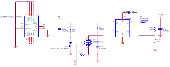
This is my inverter circuit. But when I turn on the power, pin 1 (ugate)and pin 8(phase) of tps28225 will be short circuited.At the same time, NMOS has no short circuit.
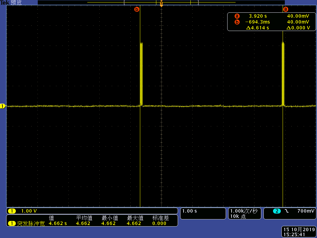
The first photo is 3.3V bus --- this is normal behavior, voltage is off during the low time and bus is high impedance slight changes in load will result in large change in low level.
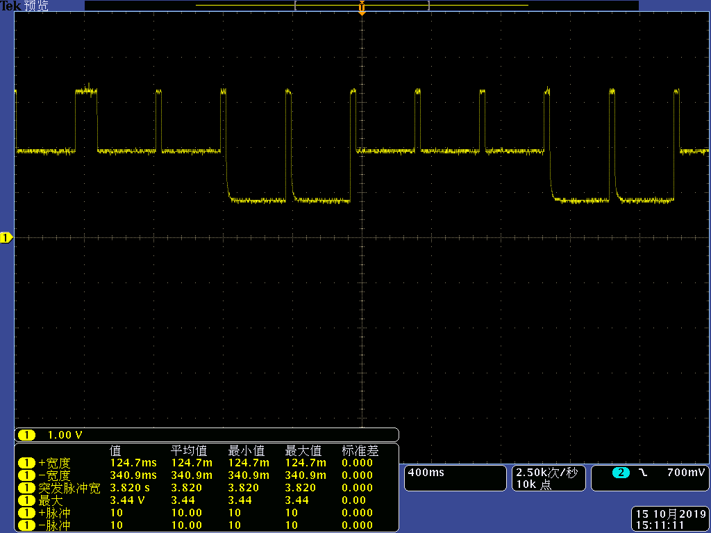
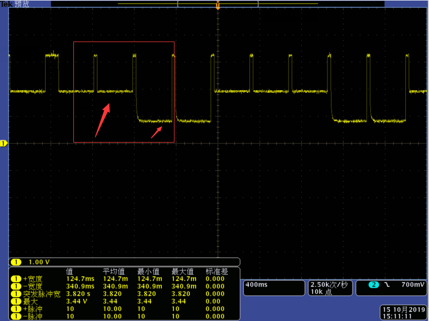
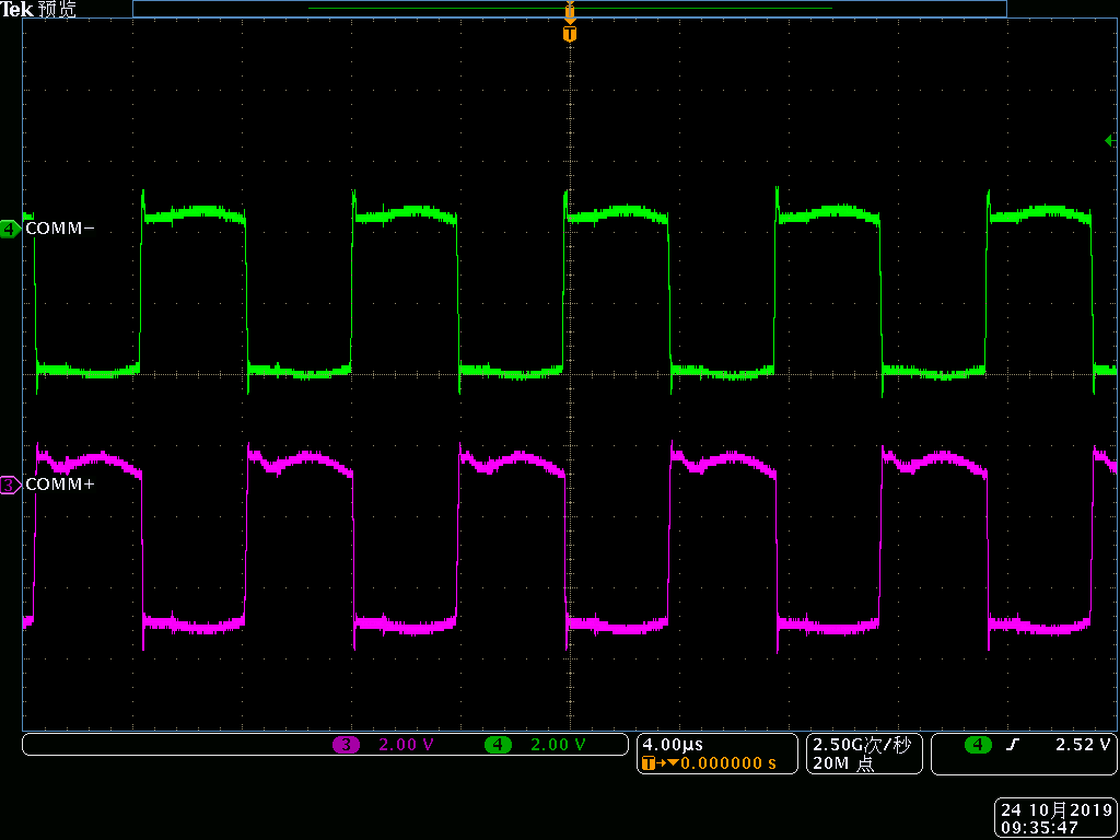
The 2ed and 3ed Comm photo -- This looks normal, comm is occurring at a about 2kHz and is modulation of the operating freq. What is captured in the scope shot is operating freq.