This thread has been locked.

If you have a related question, please click the "Ask a related question" button in the top right corner. The newly created question will be automatically linked to this question.

LP8758-E0: Vout ramps up again when shortcut is removed while EN pin is static low

Part Number: LP8758-E0
Other Parts Discussed in Thread: LP8758

Test case description

LP8758-E0 ("LP")  is used to supply 4 voltage rails.

Rail 0: 1.0V
Rail1 : 1.8V
Rail2 : 1.2V
Rail3 : 1.8V

Vin=5V

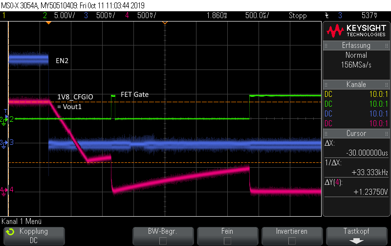
EN2 which is programmed to be enable/disable rail1. There is capacitive load of 350uF on Vout1.

Oscilloscope screenshots are available on request.

Observation1

I start to shut down rail1 by setting EN2 to 0.
Depending on the programmed slew rate Vout ramps down more or less slowly.
If configured the slew rate is too high, then the LP stops ramping down and
Vout1 starts ramping up again while EN2 is still 0 !

In order to enforce a quick shut down, I do shortcut Vout1 to GND using a strong FET.
In my test case this happens 1ms after EN2 got 0.
Vout1 immediately (20us) drops to near 0V.

After 60us the FET is switched off which removes the short cut from Vout1.
Vout1 now starts ramping up again while EN2 is still 0 !

Observation2

While EN2 = 0 and the FET is activated to shortcut Vout,
the LP draws much more current from Vin.
I looks like the LP still tries to maintain Vout1 up, even if EN2=0 and Vout already is near 0V.

LP still sources power from Vin even if  EN2 is 0 and even if Vout1 is already down.

Requirement

In my application I need to do an emergency shutdown of all power rails within 500us while using a power down sequence.

Therefore for each rail one by one I disable EN and 10us after  I do shortcut the Vout using a FET.
The Vout is forced down and the FET is kept active preventing the Vout to ramp up again.
But the LP tries to keep Vout alive for many milliseconds. This sources a high current from Vin.

During this emergency shutdown Vin itself is sourced from a capacitor bank only,
but all shortcuted LP regulator rails on board sum up to a large current at Vin which decharges the Vin capacitor bank rapidly.

My requirement is, that the LP immediately stops to draw  current from Vin when ENx is 0 and Vouts is shortcut to 0.

Best reagrds,
Ingmar

  • Hi, Ingmar,

      Since LP8758-E0 has been factory programmed to use EN1 control all power rails, if you need to use EN2 pin control rail1, please refer to and follow its datasheet section 7.3.3.1 Enabling and Disabling for more details of changing its enable control mechanism. 

      From what you described, it's most likely because the changes made through I2C are not completed properly. Please let's know if you still have issues. 

  • Hi Phil,

    Thank you for the quick answer.
    I already cross checked the I2C registers, it looks all right.

    But I will double check the schematic and layout again.
    We are going to do a board redesign, so it would be nice just to find a layout/schematic error or a bad I2C setup.

    I have measured EN2 and  Vout1 at the Oscilloscope and I can see that Vout1 immediately starts ramping down when EN2 goes low.
    So it should be the right configuration in Register 0x04 regarding EN2 control.

    When the LP ramps Vout down:  How is it realized ?

    a) Ramping down the internal target voltage reference while leaving the buck regulator enabled => Vin stays connected
    b) Turning off the high side FET while contolling the low side FET to slow down the Vout discharge => Vin stays disconnected

    Best regards, have a nice weekend
    Ingmar

    PS: Below some screen shots and the register setup...

    ================================

    The AC disortion on EN2 results from a small wire to connect the probe to the EN2 PCB trace. The EN2 signal on pcb board is 'clean'.

    The same image showing also the current (Inductor current of the main 5V Vin regulator)

    Register setup

    Reg 0 = 1
    Reg 1 = e0
    Reg 2 = 88
    Reg 3 = 3d
    Reg 4 = e8
    Reg 5 = 3d
    Reg 6 = e8
    Reg 7 = 3d
    Reg 8 = c8
    Reg 9 = 3d
    Reg a = 4e
    Reg b = 4e
    Reg c = b2
    Reg d = b2
    Reg e = 76
    Reg f = 76
    Reg 10 = b2
    Reg 11 = b2
    Reg 12 = f
    Reg 13 = f
    Reg 14 = f
    Reg 15 = f
    Reg 16 = 0
    Reg 17 = 0
    Reg 18 = 0
    Reg 19 = 0
    Reg 1a = 0
    Reg 1b = 0
    Reg 1c = cc
    Reg 1d = cc
    Reg 1e = 2
    Reg 1f = 55
    Reg 20 = 55
    Reg 21 = 0
    Reg 22 = 0
    Reg 23 = 0

    My debug console register read back decodes this  as:
    ================================
      Configuration:
        OTP Id   :  0xe0
        EN1 pdown:  0
        EN2 pdown:  0
        WarnLevel:  105C
        SprdSpec :  0
      Status:
        Th Shutd :  0
        Th Warn  :  0

    Power Rail 0: "1V0_A_GXB"
    --------------------------
      Status:
        Running   :  1
        PowerGood :  1
        I Limit   :  0
        Shorted   :  0
      Configuration:
        Voltage   :  1000 mV
        I limit   :  5000 mA
        slew rate :  1900 uV/us
        ena       :  1
        ena pin   :  0
        floor     :  0
        discharge :  1
        pwm force :  0
        delay up  :  15 ms
        delay down:  0 ms

    Power Rail 1: "1V8_A_CFGIO"
    --------------------------
      Status:
        Running   :  1
        PowerGood :  1
        I Limit   :  0
        Shorted   :  0
      Configuration:
        Voltage   :  1800 mV
        I limit   :  5000 mA
        slew rate :  1900 uV/us
        ena       :  1
        ena pin   :  2
        floor     :  0
        discharge :  1
        pwm force :  0
        delay up  :  15 ms
        delay down:  0 ms

    Power Rail 2: "1V2_DDR4"
    --------------------------
      Status:
        Running   :  1
        PowerGood :  1
        I Limit   :  0
        Shorted   :  0
      Configuration:
        Voltage   :  1200 mV
        I limit   :  5000 mA
        slew rate :  1900 uV/us
        ena       :  1
        ena pin   :  2
        floor     :  0
        discharge :  1
        pwm force :  0
        delay up  :  15 ms
        delay down:  0 ms

    Power Rail 3: "1V8_A_GXBPLL"
    --------------------------
      Status:
        Running   :  1
        PowerGood :  1
        I Limit   :  0
        Shorted   :  0
      Configuration:
        Voltage   :  1800 mV
        I limit   :  5000 mA
        slew rate :  1900 uV/us
        ena       :  1
        ena pin   :  1
        floor     :  0
        discharge :  1
        pwm force :  0
        delay up  :  15 ms
        delay down:  0 ms


  • Hi,

    This looks interesting. Schematics would be helpful here if possible to share. Anyway your shutdown requirement in 500us sounds pretty fast.

    One issue here looks to be that maximum output capacitance is limited to 50µF/output per datasheet and there is a lot of more on board if you have 350µF per output.

    Despite of excessive capacitance on VOUT1 the VOUT1 ramps down until 0.6V as expected. But after that something sources more voltage to the output. Also interesting notice is input current waveform. How voltage behaves on input side of the device? Does the input voltage go lower than specified UVLO limit 2.4V? Anyway if BUCKx is controlled by any method, pin or I2C, the disabled BUCK should not draw any current from VIN.

  • Hi,

    thank you for the reply.

       > Anyway if BUCKx is controlled by any method, pin or I2C, the disabled BUCK should not draw any current from VIN.

    This is what I would expect.

    The power supply is a two stage design:
    The main power switching regulator goes down from 24V to 5V@8A max.
    The 5V is buffered with 1800uF ceramic condensators (3700uF was a wrong info)
    The second stage consists of two  LP8758-E0  and one  LP8758-B0.
    One of the second stage LP8758-E0 voltages is 1V8_CFGIO which is buffered with about 500uF (ceramic).
    This one is shown in the scope screenshots.

    The observation of this thread came up when I verified the emergency power off sequence: Just pull the plug from 24V.

    The 24V then ramps down quickly as buffered only with 5uF.
    The primary regulator gets an UVLO. As soon a s I shoot down the second stage regulators the 5V capacitor voltage ramps down in a linear manner from 5V down to about 2.7V within 350us. This corresponds to a high constant current of about 12A drawn from the 5V rail.

    Then I investigated if the primary regulator actively discharges the 5V output capacitors while in UVLO. Therefore I measured  the current through the inductivity connected to the switching output of the first regulator (Agilent 50MHz DC current probe) . This current immediately drops to 0 when the first regulator is turned off and does not get negative. So there is no active discharge of the 5V capacitors by the first stage regulator.

    Then I investigated what happens to the second stage regulators (LP8758).
    So I triggered the emergency shut down procedure on the second stage regulators while leaving the 24V connected and the 5V regulator working.
    Furthermore I stretched the time between setting EN low and shortcutting the LP8758 Vout with a FET.

        > Does the input voltage go lower than specified UVLO limit 2.4V?

    Therefore  in the screesshots Vin=5V is alive and up due to the fact that the first stage regulator is still working.

         > Despite of excessive capacitance on VOUT1 the VOUT1 ramps down until 0.6V as expected.

    This depends much on the programmed slwe rate. If you select the fastest slwe rate of 10mV/us then the Vout only ramps down by about 0.3V.
    I didn't check if in this case Vout also ramps up again.  If you select a slower slew rate the voltage ramps down to a lower level before ist stops.
    If you select 1900uV/us and slower it ramps down to 0.6V.

      > Schematics would be helpful here if possible to share

    I have to check how we could provide schematic. For sure I'm not allowed to send them through the comunity area.
    You may connect me by email.

    Thank you
    Ingmar

  • Hi Ingmar,

    We can continue discussion with emails.