This thread has been locked.

If you have a related question, please click the "Ask a related question" button in the top right corner. The newly created question will be automatically linked to this question.

TPS61070: The TPS61070 is getting damaged very easily, don't know the reason

Part Number: TPS61070

Hi,

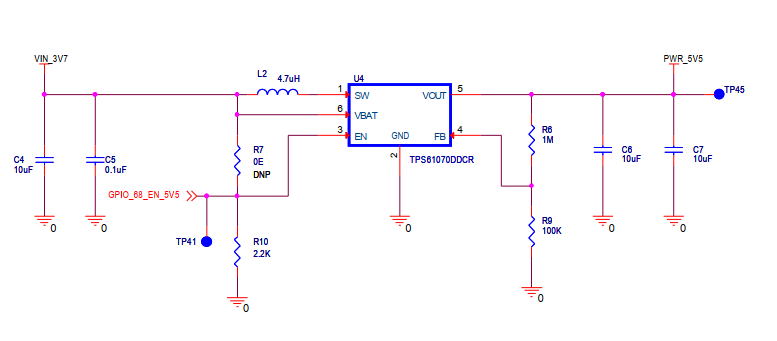
I am using TPS61070DDCR as a 5.5V supply regulator IC in my design. The input voltage is provided with a LiPo battery which has 3.0V to 4.2V supply range, the output voltage is 5.5V with less than 50mA as the output current. The regulator works perfectly for a few days then it will get damaged by showing output voltage as less than 4V eventually getting short-circuited. When I checked the temperature that appears across the IC is a maximum of 60 degrees Celcius. The load is an LCOS display and if I unsolder the TPS61070 from the pads the display will back drive the 5.5V rail with 2.7V. I couldn't find any reason for this issue, please help me to find the reason for damaging the IC? I am attaching the Schematics of the regulator with this post.

  • Hi Sajin,

    please measure the impedance between SW and GND pin, I guess this pin got damage by the SW voltage spike

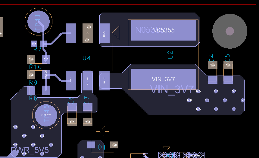
    please share your layout, the C6 should be closed to the IC.

  • Hi Sajin:

    Thanks for asking. May I know how many board you have made and how many times the issue happen.

    If the issue is not accidental , please share the layout and the part number of the inductance with me.

    Besides, I'm not understand this sentence well :"The load is an LCOS display and if I unsolder the TPS61070 from the pads the display will back drive the 5.5V rail with 2.7V." Where is the 2.7V rail?

  • Hi Jasper,

    Thank you for your reply. The impedance across SW and GND, when measured using a multimeter, is 43 ohms (Resistive impedance for the damaged IC). I am attaching the layout image with this post please check them?

    Since the load is much smaller why the SW voltage spike damaging the IC?

  • Hi Miniqiu,

    Thank you for your reply. up to 10 boards get damaged by this issue and the issue is common in every board, not an accidental. I am attaching the layout with this post, could you please check them?

    Besides, I'm not understand this sentence well :"The load is an LCOS display and if I unsolder the TPS61070 from the pads the display will back drive the 5.5V rail with 2.7V." Where is the 2.7V rail?

    Ans: The TPS61070 has only one load to drive and it is a display. The display has another 1.5V supply also, so when I remove the damaged IC from its pad and turned on the display using only 1.5V then the display drives the 5.5V from zero to 2.7V.

  • Hi Sajin,

    the device should be damaged by high SW voltage spike. the placement and routing of the output capacitor is not good. please follow the suggestion in the datasheet to modify the layout. also add a RC snubber in SW pin to reduce the peak (https://www.ti.com/lit/an/slva255/slva255.pdf )

  • Hi Jasper Li,

    Thank you for your reply. Is there any other way to solve the issue without changing the layout, because the board is a very complex one and changing the layout and manufacturing a new one is pretty in cost. If there is any way to do it without changing the layout then it will be a huge help for us

  • Hi Sajin,

    what is the status of the system board? is this your final PCB?

    you could add snubber circuit (a resistor and a capacitor) to solve the issue in current board, so the whole system can work. then modify this circuit in your next PCB.

  • Hi Jasper Li,

    The board is around final. I will check the possibility to add snubber to the design. before designing this board I already simulated the circuit in Webench and it didn't show any issue in the design

  • Hi Sajin M,

    the behavior is related the layout, which is not modeled in the simulation.