This thread has been locked.

If you have a related question, please click the "Ask a related question" button in the top right corner. The newly created question will be automatically linked to this question.

UCC28740: Ucc28740 stops every 2ms

Part Number: UCC28740
Other Parts Discussed in Thread: TL431, UCC28720, UCC28600, LM5023

Hi,

  I am having problems with a AC.DC convertor based on UCC28740 5V/3A

My VS is under 4V , CS at around 800mV and switching frequency (1A) around 30Khz

  What I observe is that every 2ms mosfet stops working. So for 2ms (around) its switching normally at 30Khz  , then 2ms it stops completely , then again in starts. Because of this behaviour , we get noise.

  What can explain this behavior ?

Vs.pdf

  • Hello User5327551,

    Thank you for your interest inn the UCC28740 flyback controller. 

    Unfortunately, there is not enough information in the files to directly diagnose the problem, but I can make a guess based on indirect information.  Since there is ~2ms between restarts and the HV pin provides ~250uA to the VDD cap, and it must rise from ~8V to ~21V in 2ms, I estimate that you have about 38nF of capacitance on VDD.    

    This capacitance may be too low to hold up the VDD while the output capacitance is trying to charge up to the point where the reflected auxiliary winding voltage can keep VDD > 8V.   

    Are you starting up into a full load?  Can you try starting with a lower load to see if it stays running?  If so, then most likely you will need to increase Cvdd so that VDD does not drop as far during the start-up interval when the load is high. 

    Regards,

    Ulrich

  • I think I found my problem .

      Is it safe to assume that Vdd needs at least 2.65mA to run  and only 0.1ma  to start ? (safer to have 5ma at all time)

  • Hello User5327551,

    Yes, your assumption is basically correct.  However, the VDD loading is only ~18uA during start-up, and the IC's maximum demand after start-up could be as high as 2.65mA to run but that does not include the MOSFET gate charge current.  Added to the controller run-current is the maximum gate charge Qg times the maximum switching frequency fSW. 

    For example, if Qg = 20nC and fSW(max) = 80kHz, then I_gate (avg) = 20nC*80kHz = 1.6mA.  So total load on VDD = 2.65 + 1.6 = 4.25mA. 
    An auxiliary winding capable of providing at least 5mA continuously will certainly do the job.  

    Regards,
    Ulrich

  • I checked , I actually have 100mA on VDD..so it cannot be the issue... what else do you suggest ?

    Is it possible that Vdd is too low at 12V ?

  • Hello User5327551,

    As seen in the UCC28740 datasheet, the UVLO turn-off threshold is 7.75V (typical), so 12V is not too low for VDD.  It is quite reasonable. 

    Since VDD does not appear to be the problem, there must be some fault condition that is detected after about 2ms of operation that is causing the controller to shutoff switching and recycle.   It could be an output overvoltage or overload condition or something. Please review the datasheet for the types of faults that the controller can detect and act on.

    I suggest to follow this debug guide to determine the problem: http://www.ti.com/lit/an/slua783/slua783.pdf .  Although it is written for PSR controllers and the UCC28740 is an SSR controller, many of the start-up issues and fault conditions are the same so this debug guide is still useful for the UCC28740.  It will help you find out what is causing the shutdowns after 2ms. 

    Regards,
    Ulrich

  • Our CS , CS and Mosfet Sw all look good.

    We tried adding 100uF on the Vdd and observe that it takes 6s to start up (much longer than before)

  • Hello User5327551,

    It is understandable that adding 100uF to VDD will cause the start-up time to increase significantly.  Presumably, this huge value is intended for testing only and not intended for permanent change.  I had suspected earlier that the 2ms timing between switching intervals may have been due to the cycling of VDD and after calculating a possible capacitance based on this suspicion, I suggested increasing the value.   Since then you indicated that VDD was ~12V, and we concluded that VDD was not the issue.  Experiencing the problem even with 100uF confirms that, so I recommend to revert back to your original value.  If you could please post a schematic diagram of the UCC28740 converter, it would help a lot to diagnose the problem.  Please include transformer inductance and turns ratios, too. 

    Please post your waveforms for VS, CS and MOSFET Vsw, showing only one or two cycles.  Your previous waveforms were at a time sweep much too slow to discern any details about these signals.  Please use a low-capacitance probe on VS.  Normal probes (with capacitance of 10~15pF) can distort the VS signal too much and affect regulation.

    Also, please include a screenshot of CS and VOUT at 1ms/div. 

    Regard,

    Ulrich   

  • OK but by using 100uF in the VDD I am able to calculate the RC time constant to charge it...and I arrive at around 40.000 Ohm (to charge the cap in 6s) and that  R indicates there is only about 0.5ma on the rail..

      Am I correct  to calculate it like that ?

  • Hello User5327551,

    At start-up, the VDD capacitor is charged up by current derived from a JFET on the HV pin, which is usually connected to the bulk rail.  This current is relatively constant (not exponential), so timing can be calculated by i/c = dv/dt.  The typical charging current through HV is 250uA.  250uA/100uF = 2.5V/s.  Inverting that gives you 0.4s/V and to go from 0V to 21V start-up threshold gives you 0.4s/V x 21V = 8.4s.  Your 6s start-up time is faster than this (assuming VDD starts at 0V), so it indicates that the HV current is somewhat higher than the typical 250uA (namely, about 350uA).   

    Regards,
    Ulrich

  • Hi Ulrich

     previously we used 22uF as Vdd capacitance , we will try tomorrow to change to 10uF (as per datasheet of TI). Do you think that more capacitance on Vdd can explain those issues ?

  • Hi User5327551,

    No, I think that VDD is not involved with the issues causing the shutdown-restart cycles.  I recommend to just keep it at 22uF from now and we'll concentrate on other possibilities.  Changing to 10uF will just add another variable into the mix that isn't necessary at this time.  VDD cap can be optimized later after all other functionality is working correctly. 

    This is where I need to review your schematic diagram, so I can look for potential sources of problems that we can investigate and debug.  I look forward to seeing one (including transformer details) as soon as you can manage it, or else progress is likely to be very slow.   The waveforms that I asked for, too, although I understand that it may take a little while to generate them.  Please send the schematic ahead of time. 

    Regards,
    Ulrich


  • Hello , this is the schematic SMPS TI.pdf

  • Do you need anything else ?

  • Hello User5327551,

    Sorry for my delayed reply.  Thank you for providing the schematic diagram and transformer spec. From these, I have a number of items to cover.

    1. Based on the turns ratio and input voltage range, operation at the high end of high-line will exceed the reverse voltage rating of your output diode D7. I recommend to replace the diode with a higher-rated schottky, or increase the P:S turns ratio to reduce the reflected voltage.  You can still debug at lower input voltages until you change the D7 situation.

    2. I’m confused by the schematic indicators and your original comments on the output voltage.   In your first posting of this thread, you indicate 5V/3A. The schematic text indicates 6V, 3A. The TL431 REF-divider calculates to 5.84V. Please clarify what the actual output voltage is intended to be.

    3. The Nps ratio of 9:1 reflects about 56V to the primary, but you have a 700V MOSFET with underutilized Vds rating. The Nas ratio of 8/5 gives you a steady-state VDD of about 10V, which is relatively close to the 8-V turn-off threshold.   I recommend redesigning the transformer to better utilize the maximum available duty cycle and increase margin to VDD UVLO. I recommend to use the UCC28740 Design Calculator Tool (www.ti.com/.../sluc487 ) to obtain the best values for all of the power stage and control parameters. If you are unable to change the transformer design, plug in the actual values used into the calculator to obtain the follow-on component values.

    4. Aside from the over-spec’d 700-V rating, the MOSFET is rated for 6A, which is oversized for the current that it must handle. While it may have very low on resistance, it consequently has very high Coss which increases turn-off delay and leads to higher peak primary currents than expected. This in turn, leads to lower switching frequencies than expected. A smaller FET with lower Coss will restore better control over the peak current.

    5. With the given turns ratios, 68K at R7 allows start-up at about 62Vrms. Is this intended?

    6. With the given turns ratios and 68K at R7, 36.5K at R8 set the output OVP level at ~8.2V. Is this intended?

    7. I recommend to

      1. delete C26 from FB to GND, and to delete C6 across the opto output;

      2. change R6 from 50R to 0R to allow C4 to charge up faster each cycle;

      3. depopulate primary snubber R41 and C25. Q2 should not need these;

      4. depopulate R51 and C74. The TL431 should not need a “soft-start”;

      5. change R40 from 2K to 1K to keep the TL431 biased better;

    8. Inductor L7 placed between a smaller C39 and a larger C40 can lead to significant low frequency undamped ringing. This may account for why you may see 12 V on VDD when the ratio indicates that only 10V should be there. I recommend to short out L7 during debug until all other testing is complete. If still necessary for ripple reduction, I recommend to change C39 to 3300uF and change C40 to 820uF. The lower impedance cap should be first after the output diode.

    9. I ‘m not sure if R4 and R5 are the correct values for your design, but the calculator tool should give you the proper target.

    10. I suggest to depopulate R12 (in secondary snubber) to remove the snubber influence to turn-on current spikes. Later, if D7 is down-sized from 20A rating, you can optimize C12 to the lowest value necessary to do the job.

    Please do what you can with these recommendations and see if your system behavior improves with stable steady-state operation over the full line and load ranges.  After that, you can concentrate on ripple reduction and noise filtering and minimizing any snubbers which may be necessary.

    Regards,

    Ulrich

  • Dear Ulrich

      your sugestion of removing the C26 made the Mosfet behave properly (ie is not stopping any longer every 2ms)

    We still have a 1.5Khz noise bumb (200uV so rather low)..any idea what can cause it ?

       In any case we are fine tuning the FB , CS.

      At last we can get only up to 2.5A (89Khz switching frequency) . AT 2A we switch at arounf 75Khz . Do you think we cannot reach 3A because SW is too high ?

    THX YOU . Great help.

  • Hello User5327551,

    I'm glad the 2-ms hiccupping has been resolved.  Please don't forget to review all of the other recommendations and comments of my previous reply. 

    I'm not sure what the 1.5kHz noise "bumb" is... I'm assuming that you meant "bump" but even so, I don't know what you mean, which signal it is or under what conditions it happens.  200uV is rather low for just about any signal.  Is this a problem?

    To get 3A output reliably, the converter should actually be designed to provide about 5~10% more current than rated.  Since the maximum frequency is 100kHz and you are already at 89kHz at 2.5A, I do believe that you will not be able to achieve 3A with the existing values of R4 and R5.   As I mentioned in my previous reply, I recommend that you fill out the UCC28740 Design Calculator Tool, using the transformer parameters that you have now, to determine the correct value for the current-sense resistor (R4||R5) at the maximum switching frequency that you specify.  This tool will also help you determine other component values, to reduce the amount of trial-and-error debug. 

    Regards,

    Ulrich

  • Hi ,

     we solved the 3A issue (by making sure that switching frequency is under 70Khz at maximum load)

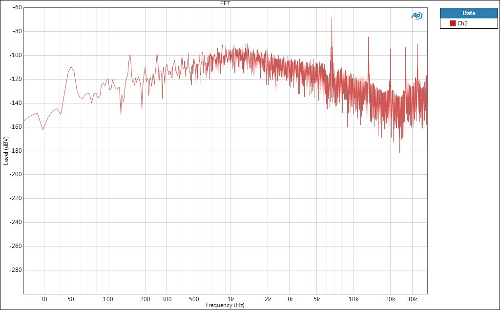
    Now I have one more issue ...as you can see attached we have a spike at 6Khz and harmonic (1A and 2A switching at 30-40Khz) .

      Any idea what can cause it ?

  • Just an update , when using 10R in Gate of Mosfet we see a reduction (6db) of 6khz noise and harmonics

  • Hi User5327551,

    I am not certain, but I believe that the 6kHz and its harmonics are sub-harmonics resulting from the built-in frequency-dithering feature of the UCC28740.  This dithering (adding some spread-spectrum to the switching frequency) operates in a repeating 6-pulse cycle.  Within this dither-cycle, the primary peak current (Ipp) level is altered slightly and the each switching period is also altered correspondingly to maintain an even delivery of energy per cycle over the 6 cycles.  This feature is not explicitly discussed in the datasheet, but is bulleted on page 1 and mentioned in Note (1) on page 6. 

    If your converter is operating at 40kHz (nominal), the 6-pulse dithering will result in a dither pattern repeating at 6.67kHz.  This then would have its own harmonics at 13.3kHz, 20kHz, etc.  I believe that this is what you are detecting with the FFT scan.  I expect that this kind of harmonic pattern would track the nominal frequency at different load levels.  I'm not sure why the 10R gate resistor would reduce the peak magnitudes.  

    Note: at some lower load level, the dithering feature is shut off.  (In this state the switching frequency and Ipp stay constant for a constant line and load.)  The shut-off occurs somewhere near the lower-FM/AM region boundary of the Control Law curve on page 16 of the datasheet.  There is some hysteresis in the feature, so after dithering is shut off, it stays off until the load is increased somewhat higher up in the AM region.  I don't know the exact points where dithering is stopped or resumed. 

    Regards,
    Ulrich

  • Anyway to have a way around it ? It creates more problem than solving (EMI.)

      How about if I move the SW frequency around 28Khz...it will be disabled  ?

    ANy other way to move this noise out of audio band (20Khz)

     AT 3A and 54Khz switching noise is moving to 8.2Khz.. and harmonic.

  • Hello User53275551,

    The frequency-dither feature is not adjustable.  It is theoretically possible to design the converter to operate at 3A output at frequencies below 28kHz to disable the dithering but this will severely de-optimize the transformer size and overall efficiency, and I think it will result in a current limit much higher than 3A.  I think it will also result in a much higher minimum load requirement to avoid OVP at no-load (due to the 170-Hz minimum switching frequency).
    I do not recommend this course of action.

    Your FFT graph is labeled in dBV, and the peak signals are all well less than 1mV (-60dBV).  What voltage is being measured?  Is this measured at the output or the input; common mode or differential?   

    What problem is being created?  Do you actually hear audible noise at these harmonic frequencies?  If so, which component(s) is it coming from? There may be a different way to solve the problem, depending on what is making noise.

    Regards,
    Ulrich

  • Hi

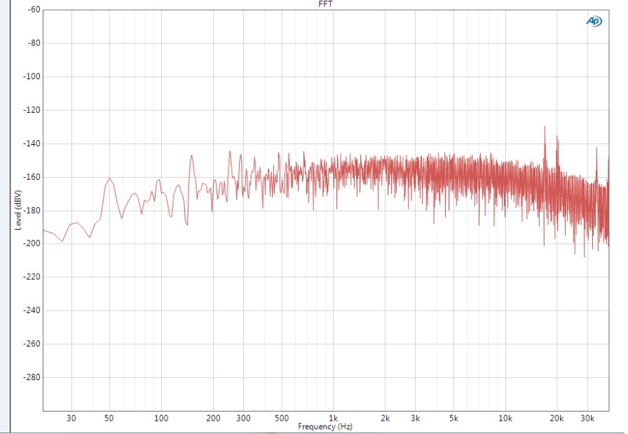
    We are able to have a load of 0.8A switching at 26Khz (stable , no dithering)  . Noise on the system is amazingly good at around 5uV

      Please note that we design this PSU as a ultra low noise PSU and noise is very important to us and our customers .

      As soon as we go to load 1A , switching frequency is between 26-32Khz and of course noise is back .

    What can we do to keep dithering out at least up to 1.5A ? Any changes in VS , CS or even FB (maybe use a different CTR opto feedback)  levels  that will allow it ? We can live with dithering above 1.5A

     At last , we are thinking that we could move to IC 28720 that seems it has no frequency dithering and its almost pin to pin (without the FB)

      This has been very helpful we have been looking for an answer for the past months. I will close the thread after your answer, with my many , many thx!!

  • Hi User5327551,

    The UCC28720 controller is possible, since it does not have the dither function, however it works with primary-side regulation (PSR) which uses the reflected output voltage on the auxiliary winding to regulate.  So it will not have as accurate of output regulation.  More like +/-5% rather than +/-1% from the SSR scheme.  Also, it is designed to drive a BJT, not a MOSFET, if that is a concern.

    Staying with the UCC28740 will require moving the 1.5A load point to below the AM frequency (32kHz) to keep the dither off.  The constant current regulation (basically the current limit) only works in the upper FM region.  Since the control law has a 4:1 Ipp range through the AM region, output power goes as Ipp squared, or 16X more.  For a fixed voltage, you won't get a CC limitation until Iout reaches 16 x 1.5A = 24A!  It won't really get that high because the rest of the power train cannot support that total power, but one also doesn't want to find out where everything collapses, either.  It will vary with line voltage.

    I don't think trying to work below the dither point is going to be practicable.  If you don't already have a post L-C filter, may I suggest trying to attenuate the harmonics?  If you do have one, maybe it can be modified to attenuate more. 

    Other options are to consider the UCC28600 flyback controller, or LM5023.  Neither have the built-in HV start-up, though.  If a really strong business case can be made, TI could develop a custom version of the -740 without dithering.  I'm afraid that I'm out of additional ideas, but I'll ask internally if there are other options.

    Regards,
    Ulrich 

  • Hello ,  I would prefer to work with the Ucc28740

       Do you know with whom I should talk regarding a custom version of the IC ? I know that qty will have to be high , but how high..

     I am attaching what I currently achieve on 1A (rather 0.9A) whitout dither. Note this is the quietest SMPS in the ..world.

       OK let me know if anyone knows of a solution and please ask someone to contact me for a custom solution .

       Again...I want to stress that rarely I have seen such outstanding support. Thx you Ulrich .


  • Hello

     any solution ?

  • Hello User5327551,

    Since we are pursuing this further through private email and the original issue has been previously addressed, I will close this thread.

    Regard,
    Ulrich