Other Parts Discussed in Thread: UCC28700
Hi Eric,
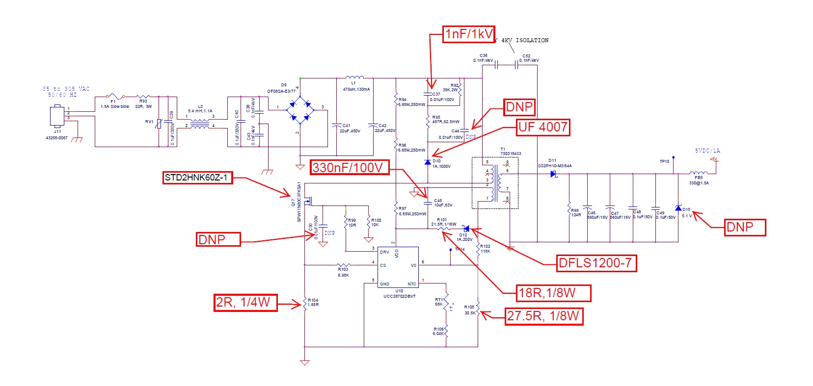
We redesigned our transformer and the basic functionality of circuit is working fine.
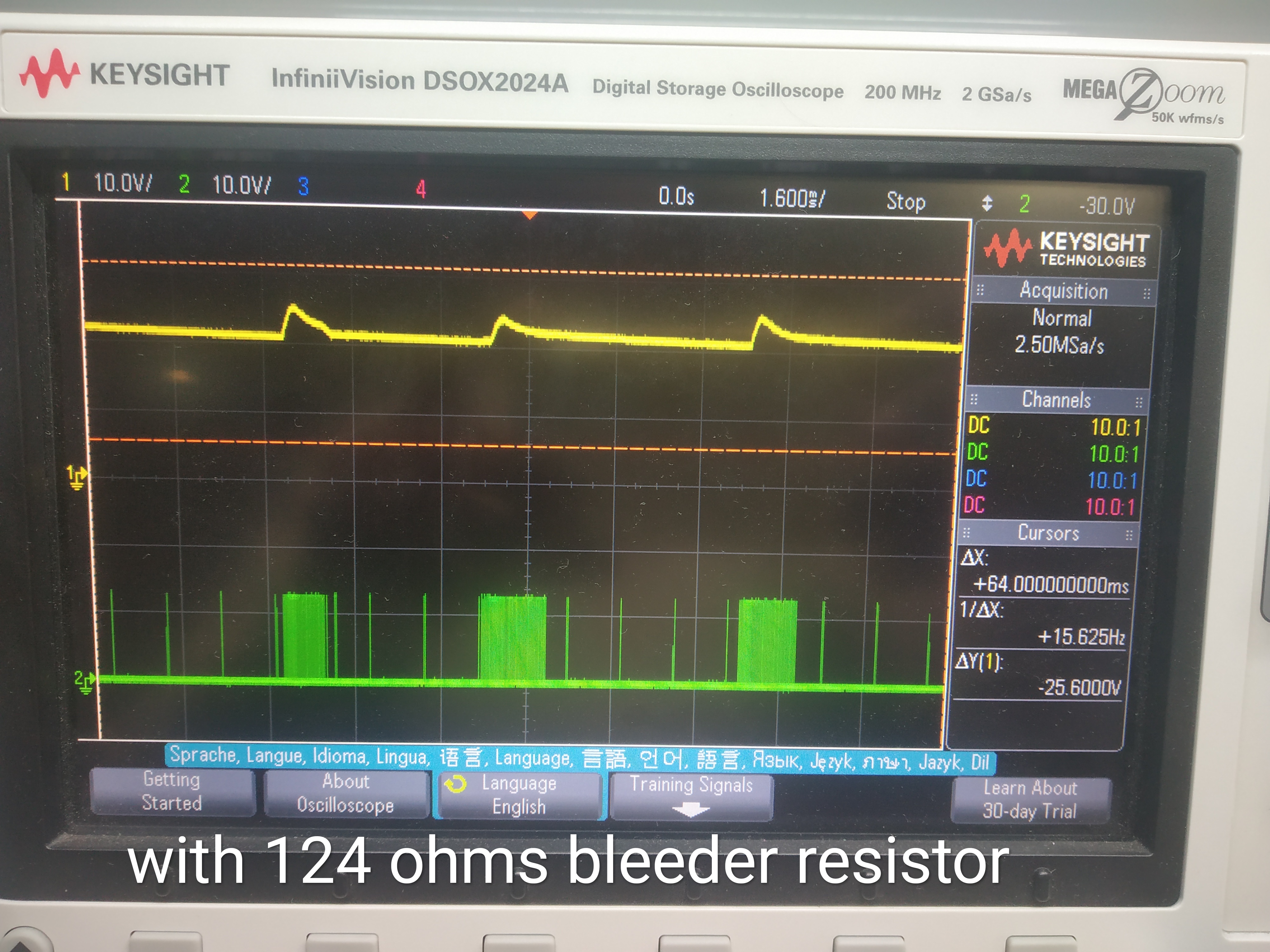
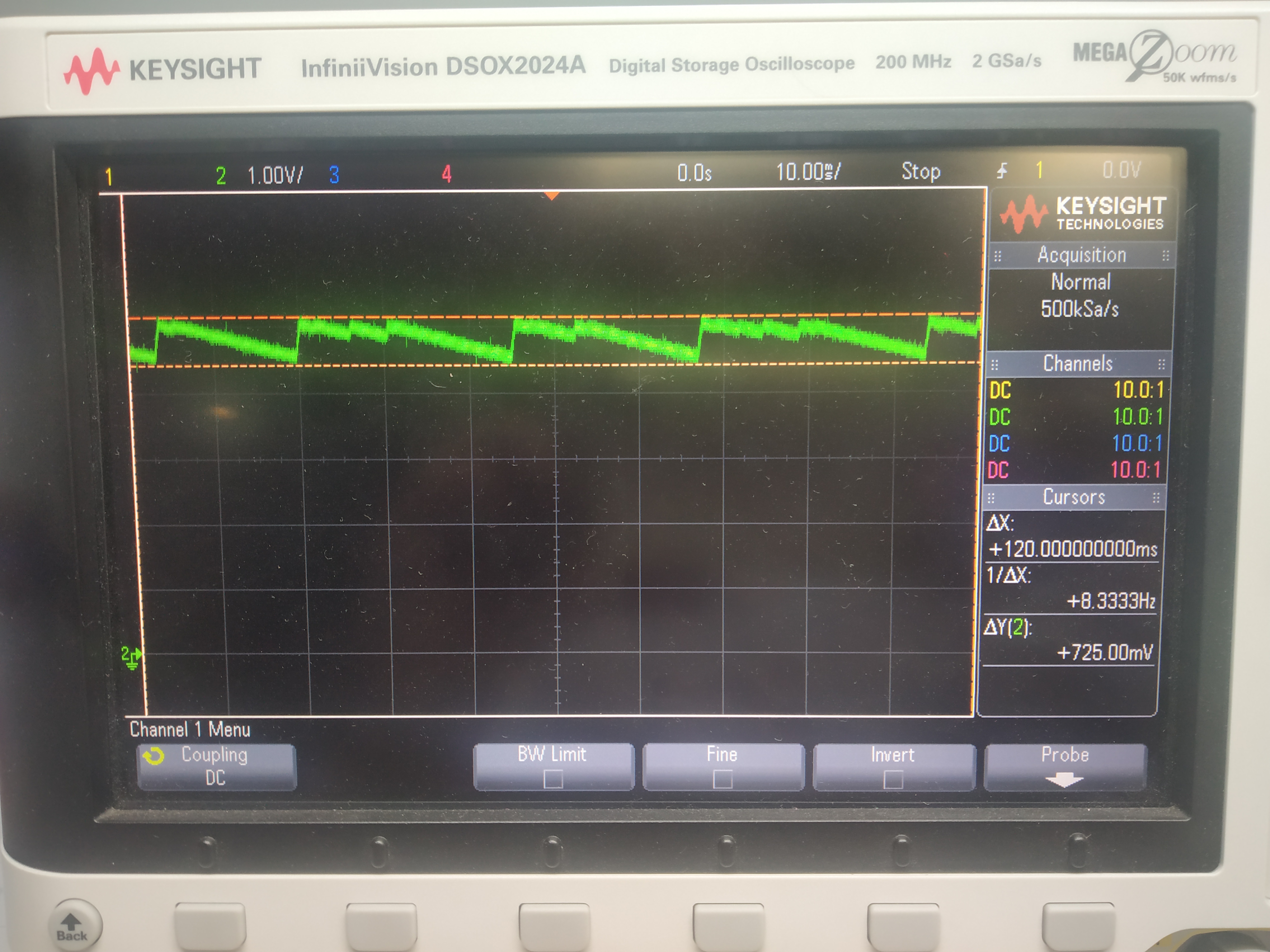
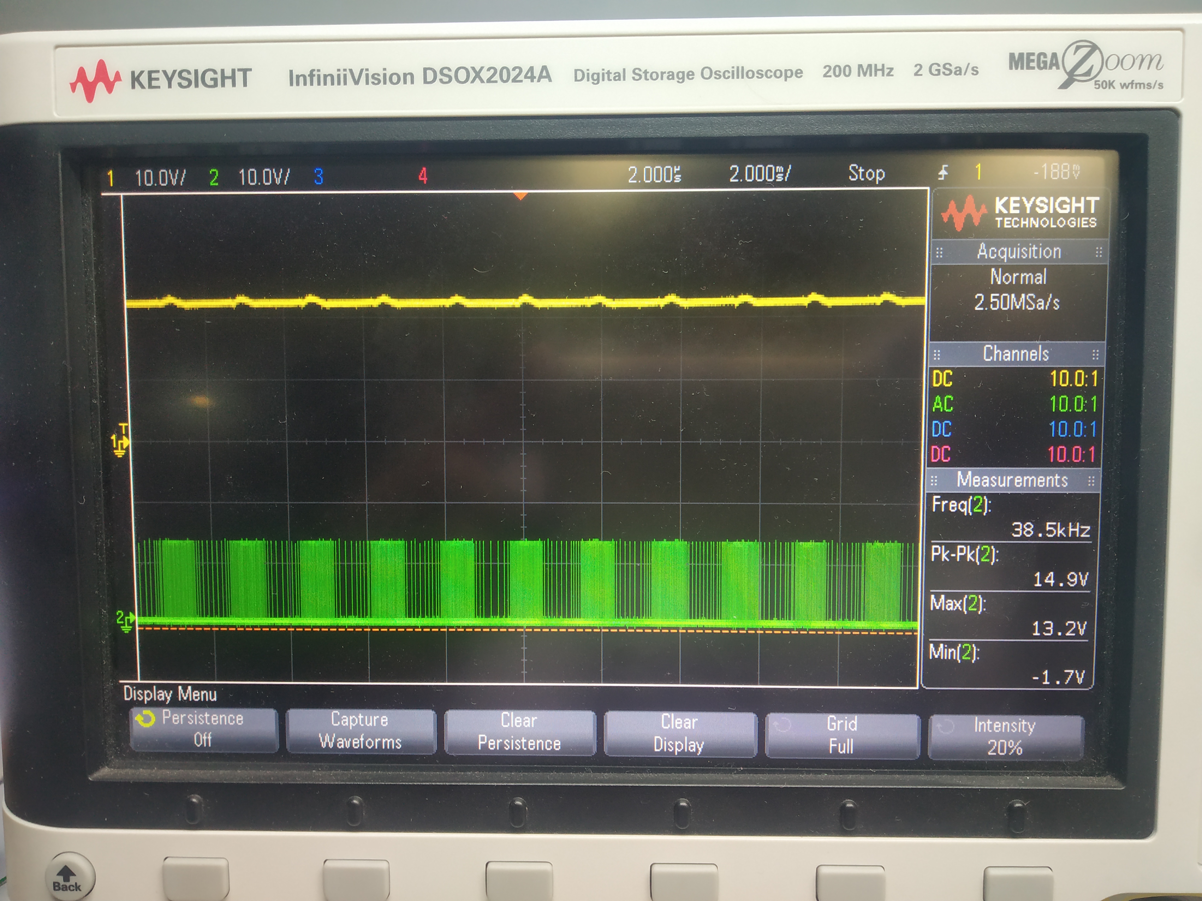
We tested entire input range from 85 to 305V AC and current from 250mA to 1A and is working perfectly. But we facing issue with lower currents below 150mA, the output voltage is continuously fluctuating between 4V to 5V in particular input voltage ranges like 170V AC to 240V AC and above 270V AC.
Can you please suggest and guide us in this regard.
Thanks in advance.
Ramgopal.