This thread has been locked.

If you have a related question, please click the "Ask a related question" button in the top right corner. The newly created question will be automatically linked to this question.

TPS65185: No communication over I2C and no voltages being produced

Part Number: TPS65185
Other Parts Discussed in Thread: USB2ANY, IPG-UI

Hello,

I am currently prototyping with the TPS651851 that I am controlling with an ESP32 and I am unable to communicate with the chip over I2C. I have a board built and I am able to communicate with the other I2C chips, but the TPS651851 does not respond to any I2C communication. Since it is a prototype, I realized that I had made a few mistakes with my design initially, so I have a few bodge wires, but testing with a voltmeter and scope it seems like at the very least I should have all the power and communication lines working correctly. I am planning on getting another board built soon to fix my known issues, but since I have not been able to test the TPS651851 I am worried that the new design wouldn't work either. The schematic that I am currently using for the chip is this:

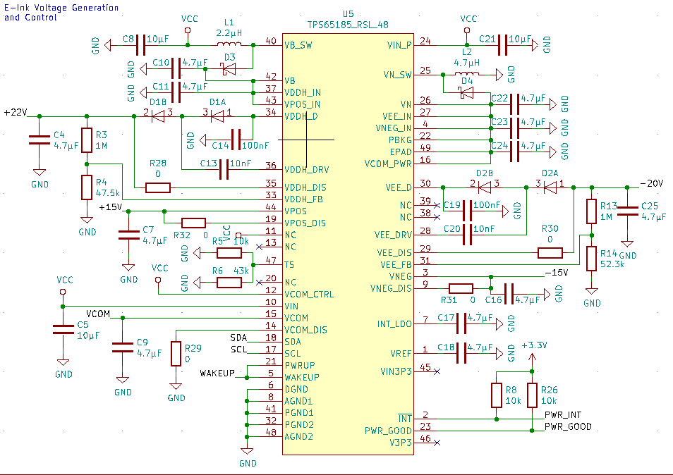
As what I assumed was the bare minimum to get communication working, I have verified that SDA and SCL are connected to the pads for the chip. Also, WAKEUP is 3.3V, VIN is 4.2V, and every ground pin is at ground. Are there any obvious issues with the design I currently have? Also, could this be a layout issue which would be a little harder to diagnose?

Finally, as I was reading through the questions on this site, I saw one saying that you couldn't leave PWRUP tied to GND in order for the chip to function correctly. From reading the datasheet, it seemed like PWRUP should be able to be tied to GND as any function it has occurs on positive or negative edge triggers and that you should just be able to use I2C commands instead. The only reason I am asking this is because I do not have enough pins on my microcontroller for a PWRUP pin, so I have it connected to WAKEUP at the moment as suggested in the datasheet, but I would prefer to have finer control rather than off and on and producing voltage.

Thanks in advance!

  • Hi,

    Looking at the schematic I do not see any immediate issues. VIN and WAKEUP are all that are required to be present to enable I2C communication with the device. I am assuming SCL and SDA are pulled up in a different part of the schematic, is that correct? Do all the rails come up correctly once WAKEUP and PWRUP are pulled high? Please provide a scope shot of power-up if possible. Keep in mind that there is also a minimum delay of 1.8 ms after WAKEUP is pulled high before the device will accept I2C transactions. Is this delay requirement being met during your power-up sequence? 

    If the device is otherwise behaving as expected, and you are able to observe the SCL and SDA waveforms at the pins of the device, my first thought would be that this is not a layout issue. Can you also provide a scope shot of your SCL and SDA waveforms when sending an I2C command? Have you verified that all the I2C timing requirements (Section 7.6 and Figure 1 of the datasheet) are met?

    If everything mentioned above looks fine, I would recommend swapping out the device to see if the unit has been damaged or if this is a systematic issue. If it is systematic, the next step, if possible, would be to attempt communication with a USB2ANY and our IP-GUI, found at the links below. These are used for internal applications validation and debugging with this device. 

    USB2ANY: http://www.ti.com/tool/USB2ANY

    IPG-UI: http://www.ti.com/tool/IPG-UI

    Thanks,
    Gerard 

  • SCL and SDA are pulled up in a different part of the schematic. Currently, none of the rails come up when both WAKEUP and PWRUP are pulled high. I am meeting the 1.8ms delay as right now I'm just using the microprocessor as a i2c console interface so I'm running commands long after WAKEUP has been pulled high. Here is a scope shot of my I2C waveform:

    The top/blue waveform is SDA and the bottom/red waveform is SCL. I am running the I2C bus at 100KHz, so I should be meeting the timing requirements and three other I2C chips are functioning correctly on the same bus.

    Since there doesn't appear to be anything wrong with my schematic, I'll probably get a few more chips to make sure I didn't damage them while putting the board together. 

    One final question though, is it okay to tie PWRUP to GND and only use the I2C commands to switch between ACTIVE and STANDBY mode? Reading through the datasheet I don't see any reason why that would not be allowed, but another answer on the site seemed to contradict that and I wanted clarification.

    Thanks.

  • Hi,

    It is possible to only use I2C commands to switch between ACTIVE and STANDBY, but if you plan to do this do not tie PWRUP to ground for the reason mentioned in the thread (https://e2e.ti.com/support/power-management/f/196/p/572040/2099706). If the functionality of PWRUP is not needed, the pin should be pulled up to an external rail, or alternatively it can be tied to WAKEUP.

    Please feel free to post again if you continue to have trouble communicating with new chips or have any further questions.

    Thanks,

    Gerard