This thread has been locked.

If you have a related question, please click the "Ask a related question" button in the top right corner. The newly created question will be automatically linked to this question.

LM5104: Wrong signal when connect to mosfet

Part Number: LM5104
Other Parts Discussed in Thread: LM5106, LM5105

Dear engineer:

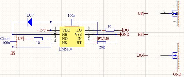
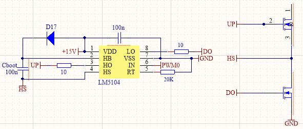
I meet a problem when using LM5104. Let me express the condition.

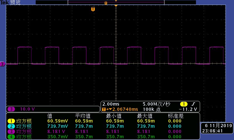
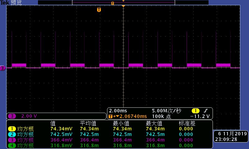
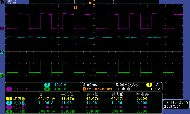
When the pin LO is not connected to the gred of a mosfet, it's output wave is right(P1). But  as soon as i connect it to a mosfet with a 10Ω driving resistance,the output wave is wrong(P2).

When the pin IN is connected to gnd, according to the datasheet, the driving signal should be 1,and it is really 1 when LO is not connected to the gred of mosfet. but it becomes 0 when LO is connected to the gred of a mosfet.

Thanks for your help.

Li Yang

  • Hello Li,

    Thank you for the interest in the LM5104. The LM5104 is a half-bridge driver configured to drive the high side MOSFET and low side MOSFET with the low side driven complementary (inverted) from the PWM input.

    I see in the second waveform the signal is not as high as expected, but it looks like it is going to some level above ground. There could be something in the circuit that is causing this behavior. Are you operating the driver with the power train connected with only the low voltage applied to the driver and no high voltage or load on the power MOSFETs?

    Can you confirm a few things. Can you confirm that the high side MOSFET gate drive is as expected? Since this driver is adaptive drive, where the MOSFET Vgs is monitored to control the dead time, if both drivers are not switching as expected it may affect the dead time timers.

    Test the driver with MOSFETs connected with only the low voltage driver and PWM input, No high voltage on the MOSFETs. Connect the switch node to ground to be sure the  HB bias is charged. Then confirm the HO and LO outputs.

    If that does not help, or if there is still issues, please provide a schematic so I can review and give additional comments.

    Confirm if this addresses your concerns, or you can post additional questions on this thread.

    Regards,

  • Dear Richard:

    Thanks for your reply. I am sorry for my less detailed discription and i will express my problem exactly. According to the datasheet, i build the Circuit.

    PS: Vds=0

    1.When nothing is connected to Mosfet, the output of pin LO is right.

    2.When DO is connected to a Mosfet, signal of the Mos‘ GS becomes wrong.

    3.When DO, HS, UP is connected to Mosfets. In this circumstance, the signal of Vgs of the up Mosfet is right but the down Mosfet's is wrong. By the way, according to your suggesstion, when connecting the switch node to ground, waveform of Vgs-up is right.

  • Dear Richard:

    I feel very sorry that the reply just now cannot disply images. So i send a new one.

    Thanks for your reply. I am sorry for my less detailed discription and i will express my problem exactly. According to the datasheet, i build the Circuit.

    PS: Vds=0

    1.When nothing is connected to Mosfet, the output of pin LO is right.

    2.When DO is connected to a Mosfet, signal of the Mos‘ GS becomes wrong.

    3.When DO, HS, UP are connected to Mosfets. In this circumstance, the signal of Vgs of the up Mosfet is right but the down Mosfet's is wrong. By the way, according to your suggesstion, when connecting the switch node to ground, waveform of Vgs-up is right.

    Violet: waveform of Vgs-up

    Blue: waveform of Vcboost

    Green: waveform of Vgs-down

  • Hello,

    Thank you for the more detailed waveforms and schematic. It appears the HO output and timing seeing the LO rising to some lower level seems correct.

    The LO output seems like it is being limited to a low level by something in the circuit. Can you confirm the connections and make sure there is not some unintended low resistance at the low side MOSFET gate? Disconnect the driver LO to the low side MOSFET gate and connect a DC supply source of 10V to the MOSFET gate and source. Confirm if there is very low current flowing with the 10V applied to the MOSFET gate to source.

    You may want to confirm the LM5104 with a new device installed, if the MOSFET gate and source are confirmed to be high resistance/low current.

    Confirm if this addresses your concerns, or you can post additional questions on this thread.

    Regards,

  • Dear Richard:

    According to your suggesstion, I disconnect the driver LO to the low side MOSFET gate and connect a DC supply source of 10V to the MOSFET gate and source. Voltage of Vgs is right(10V) and there is very low current flowing with the 10V applied to the MOSFET gate to source. The same phenomenon appears when the DC supply source of 10V is connected with a 10Ω  driving resistance. This may show that there is not some unintended low resistance at the low side MOSFET gate.

    PS: Can you recommend some drivers with low Dead-Time and they should have single-input and double-output.

    Thanks for your patience.

    Regards,

    Li yang

  • Hello Li,

    It is still not clear what is limiting the LO output amplitude in your circuit testing.

    Regarding the question on other drivers with single input and two output with low dead time, there are similar devices to the LM5104 which are the LM5105 and LM5106. These two drivers have a dead time programming pin to allow setting the dead time.

    How low of a dead time are you wanting to achieve? The LM5105 and LM5106 show dead time settings as low as 80-100ns.

    The datasheets of the LM5105 and LM5106 can be found below.

    https://www.ti.com/lit/ds/symlink/lm5105.pdf

    https://www.ti.com/lit/ds/symlink/lm5106.pdf

    Confirm if this addresses your questions on you can post additional questions on this thread.

    Regards,