This thread has been locked.

If you have a related question, please click the "Ask a related question" button in the top right corner. The newly created question will be automatically linked to this question.

LM5109B: application

Part Number: LM5109B
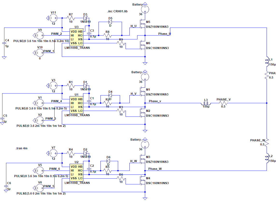
Other Parts Discussed in Thread: CSD18537NKCS

I'm using three IC to drive three half bridges to control and power the BLDC. But everytime the driver circuit was connect to the motor and microcontroller, the ICs and FETs will be broken. Is there any possible reason for this problem?

The circuit I used is same as the circuit in  the typical application.

  • Hello Can,

    Thank you for the interest in the LM5109B. There are a number of conditions that may cause overstress to the gate driver which can lead to damage to the devices.

    I would 1st confirm that the voltage on the IC pins are within the device ratings such as VDD to VSS of 8 to 14V, HB to HS less than 14V, HB to VSS < 90V. Confirm that the timing to the power MOSFETs is correct so that there is dead time between the LO output and HO output, and also the high side Vgs and low side Vgs.

    Can you operate the control and gate drive with no voltage applied to the Power FET half bridges, or with lower voltage applied to confirm the control, driver and half bridge switch node waveforms?

    Many times, voltage overstress is caused by high dV/dt switching which may result in high voltage spikes on the MOSFET switch node. This may overstress the driver HS pin. Try increasing the gate drive resistance, and confirm there is still adequate dead time on the high side and low side MOSFET Vgs.

    I can provide better advice if you can send scope waveforms of the application, and also schematic of the driver and MOSFET power stage.

    Capture scope plots of LO, HO-HS and HS to ground. Also LI, HI, LO and HO-HS will be helpful.

    Confirm if this addresses your questions, or you can post additional questions on this thread.

    Regards,

  • This is my schematic, could you please let me know if I need to add any protection to my circuit or what part of the circuit is making mistakes? Since my circuit is broken right now, I have to wait until my order come in to show you the scope image.

  • Hello Can,

    Thank you for providing the schematic. I see that the BSC160N10NS3 is relatively low gate charge of 19nC which is an effective capacitance of 1.9nF. The boot capacitance of 100nF is adequate to charge the MOSFET Qg. But since motor drive is low frequency, refer to Section 8.2.2.1 in the LM5109B datasheet to confirm the boot capacitance with the operating frequency.

    Also since the MOSFET Qg is fairly low for many motor drive applications, you may want to increase the gate resistance to 20-30 Ohms for initial testing since the 10 Ohms and 19nC is a time constant of only 19ns.

    Confirm if this addresses your concerns or you can post additional concerns on this thread.

    Regards,

  • Thank you very much for your reply. And sorry about the confusion, I was using CSD18537NKCS for my MOSFETS rather than BSC160N10NS3. Besides, is there any protection I can use on my circuit? Since the motor is really inductive, I'm worried about when the power is cut off, there will be a high voltage generated from motor and applied to HS node. I'm wondering if I can apply any protect circuit on my circuit to protect my IC and FETS.  Also, for the time constant, am I supposed to use a time constant longer than 19ns or shorter than 19ns?

  • Hello Can,

    To protect the IC from possible transients on the switch node, there is a common method used to limit possible negative voltage spikes on the driver IC switch node.

    Add a resistance in the connection from the MOSFET switch node (HS source and LS drain) to the driver HS pin. I would recommend an initial value of 5 Ohms for this resistance. Also add a Schottky diode from the driver IC HS pin to the VSS (ground pin). Locate the diode close to the IC pins to be most effective to limit the HS negative voltage.

    If your input is 36V, you should have margin for the positive HS voltage spikes since the IC is rated for 90V.

    Since you are having trouble with the operation, I would recommend increasing the gate resistance to 30 Ohms range as an initial value. Since this is low frequency operation it will be OK for initial testing. After operation is confirmed, the gate resistance can be reviewed if you desire faster switching while making sure the power train switching voltages are acceptable regarding voltage spikes.

    Confirm if this addresses your questions or you can post additional question on this thread.

    Regards,