This thread has been locked.

If you have a related question, please click the "Ask a related question" button in the top right corner. The newly created question will be automatically linked to this question.

TPS63020: TPS63020 oscillator frequency questions

Part Number: TPS63020

Hi, Ti power management experts,

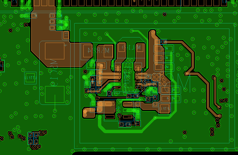
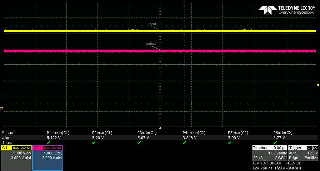
We used TPS63020 to provide LTE power. Input voltage is 5V and output voltage is 3.8V. We disable power saving mode by PS/SYNC pin pull up 100K ohm to Vin.

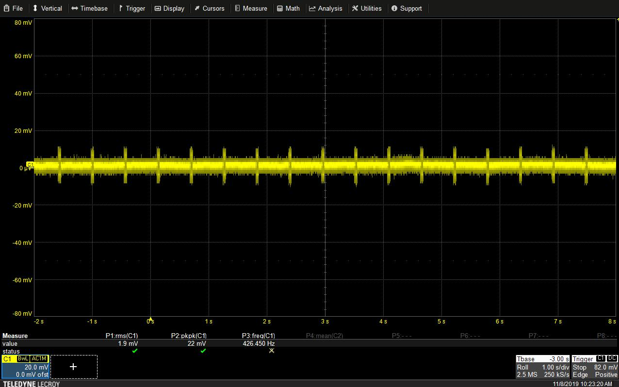
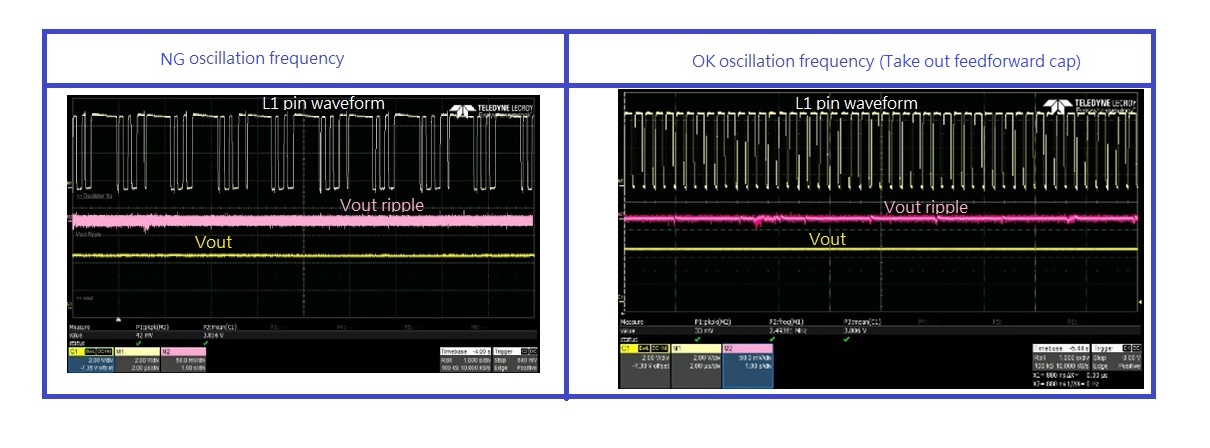
As above, I think oscillator frequecy should be fixed around 2.4MHz and duty may variate by LTE loading. I found one strange symtom that frequency may change to 820KHz sometimes when device runs under -20 degree C temperature. I don't know if it enters power saving mode. Is there any meachanism or cause that TPS63020 possibly operates at this ffrequency? When TPS63020 operates around 820KHz, the output voltage ripple also becomes a little bigger and also FB voltage is around 40mV bigger than normal frequency.

Thank you in advance for the answer.

Sincerely,

Denny


  • Hi Danny,

    This should not happen, and the switching frequency should be constant in forced-PWM mode.

    Could you please:

    1. Verify that this happens with more than one unit. For example there might be a cold solder joint on the problematic board, that causes this issue at low temperatures.
    2. Verify that the PCB layout guidelines from the datasheet are followed. 
    3. Verify that the minimum output capacitance is present when the temperature derating is included.

    Moreover, it would help us if you could send us the schematic, PCB layout and the scope plots when the device is not working properly. For the schematic and the PCB layout, you can show us only the parts around the TPS63020.

    Best regards,
    Milos

  • Hi, Milos,

    Thank you for your quickly answer. Please refer the following my reply.

    1. TPS63020 power circuit:


    2. PCB ayout

    3. Abnormal scope waveforms (f=828KHz)

    By the way, inductor and capacitor value may be decreased due to low temperature. I wonder if they are related and waht the IC internal works in theorem to cause frequencyvariation.

    Thanks in advance for the support.

    Sincerely,

    Denny


  • Hi Denny,

    If I see it correctly, there are only 1 µF and 0.1 µF ceramic capacitor on the output of the converter. The 330 µF capacitor is likely an electrolytic capacitor? As the minimum, we recommend 2x 22 µF ceramic capacitors. 

    Can you please try adding more ceramic capacitors as close as possible to the output of the TPS63020?

    Best regards,
    Milos

  • Hi, Milos,

    Thank you for your recommend. I will try it. More thinking, if output capacitors are not enpugh, can I detect regulator output stability by checking phase margin and gain margin in bode diagram?

    Thanks in advance for the support.

    Sincerely,

    Denny

  • Hi Denny,

    Yes.

    The best way is to use a network analyzer:
    https://www.omicron-lab.com/fileadmin/assets/Bode_100/ApplicationNotes/DC_DC_Stability/App_Note_DC_DC_Stability_V3_3.pdf

    If not available, a load transient test can be used, as described here, section 2.2:
    http://www.ti.com/lit/an/slva289b/slva289b.pdf

    Or you can do it with an oscilloscope:
    http://www.ti.com/lit/an/snva364a/snva364a.pdf

    Best regards,
    Milos 

  • Hi Denny,

    Is there any update, were you able to resolve your problem by adding more capacitors?

    I have some additional questions:

    1. Which signal did you show on the scope plot? Voltage on L1 pin maybe?
    2. When that signal was measured, what were the input and output voltages? 

    Best regards,
    Milos

  • Hi, Milos,

    Yes, it can be great improved by adding additional 47uF capacitor at output power.

    Regarding your questions:

    1. You are correct. I measured it at L1 pins of TPS63020.

    2. Input voltage is 5V and output voltage is 3.8V

    I have other question as the following.

    - When issue happened, we still can see the abnormal waveform of oscillation frequency without system loading. We measured the FB pin ripple waveform as the following figure. We wonder if FB pin ripple cause this issue. Even we fixed IC in PWM mode, it is possible to cause frequency shift. If output capacitor is not enough, is it reasonable to cause this issue?

    Thank you in advance and continuously support.

    Sincerely,

    Denny 

  • Hello Denny,

    1. Please measure L2 pin as well.

    2. Please measure the input and output voltage as close as possible to the IC. It is possible that the input voltage drops directly at the IC due to some effects in the system if you cool the system down.

    3. It is possible that your measurement shows GND noise instead of noise on the FB pin. It is very hard to distinguish the difference, especially when you need to get somewhat further away with the probes from the IC because of the low temperature setup. Hopefully the results of points 1 and 2 give us some more insight here.

  • Hi, Brigitte,

    Thank you for your reply.

    1. Please check the following figures for L2 pin waveform.

    - It is NG waveform when oscillator frequency is shift. L2 has pulse drop.

    - It is OK waveform when oscillator frequency is fixed. L2 is stable.

    2. We measured input voltage (Pin 10, 11) and output voltage (Pin 4, 5). There was no voltage drop symptom when issue happened.

    Thank you in advance and continuously support.

    Sincerely,

    Denny

  • Hello Danny,

    You need to have a look on the inductor current or both switch nodes at the same time to measure the frequency. The waveform of 1 switch node is not enough.

    It seems that the IC needs to operate in buck-boost mode when you cool it down, to keep the output voltage.

    This could be for example caused by an increase in losses in the external components. Please observe the input current when you cool the system.

    BTW, which method are you using for cooling?

  • Hello, Brigitte,

    Thank you for your reply.

    We measured the device in the chamber with setting -20 degree C. We soaked the device 1 hour in the chamber then we took out the device outside, boot up the device and measured waveform and function.

    Today we measured L1 and L2 at the same time as the following figure. C1 in yellow is L1 pin and C2 in red is L2 pin.

    As you said, IC seems to operate in buck-boost mode. Q1 is for buck mode and Q3 is for boost mode in the following spec figure. Generally speaking, operation mode is judged by Vin and Vout voltage. If Vin >Vout, IC operates at buck mode. If Vin<Vout, IC operates at boost mode. I wonder if any other factor will cause operation mode control error.

    In the spec 7.1 it says "to avoid ground shift problems due to the high currents in the switches........" I wonder if it will cause the problem that I have.

    I will measure input current for your reference later.

    Thank you for your kindly feedback and continuously support.

    Sincerely,

    Denny

  • Hello Denny,

    Please measure the input and output voltage after cooling the device on MSC1 and MSC198.

  • Hi, Brigitte,

    Thank you for your quickly reply.

    Please check the following figures.

    1. Input and output voltage after cooling the device on MSC1 and MSC198.

    C1 in yellow is input voltage;

    C2 in red is output voltage;

    2. L1 pin, L2 pin and input current in abnormal symptom.

    C1 in yellow is L1 pin waveform;

    C2 in red is L2 waveform;

    C3 in blue is input current waveform.


    3. L1 pin, L2 pin and input current in normal symptom.

    C1 in yellow is L1 pin waveform;

    C2 in red is L2 waveform;

    C3 in blue is input current waveform.

     More information for your reference. There is compensation circuit in FB design. We tried to remove compensation circuit and it also improved.

    Sincerely,

    Thank you for your continuously support.

    Denny

  • Hello Denny,

    Please detail how many boards you tested.

    What exactly do you mean with the information that the removal of the additional compensation components improved the behavior?

  • Hello, Brigitte,

    I test over 100 pieces of boards. 90% of the boards have this issue under low temperature. We also designed compensation circuit with same value as application circuit.

    After I removed C4 4.7pF, the oscillation frequency became stable and kept about 2.4MHz. I am also trying to figure out if PGND soldering status or PCB layout  will cause this issue or not and relationship in theorem. 

    Thank you for your continuous support,

    Sincerely,

    Denny 

  • Hi Denny,

    Could please tell me where exactly on your PCB you measure the current in your posted picture.

    Here is a scopeplot for your reference , which I measured @25degC.

    Thanks,

    Moritz

  • Hello, Moritz,

    I measured inductor current at L1 pin (separate pad and inductor).

    Thank you,

    Sincerely,

    Denny.

  • Hi Denny,


    ok, i thought this was your input current, but that makes more sense.

    Can you please restate which problem you are having? Do I understand correctly, that you have improved the regulation by taking out the feedforward cap in the feedback resistor network? 

    Regards,

    Moritz

  • Hello, Moritz,

    Yes, your understanding is correct. After I removed cap in the feedback resistor network, the oscillation frequency became normal as the following figure.

    Thank you for your continuous support.

    Sincerely,

    Denny


  • Hi Denny,

    Happy to hear that.

    Do you have further questions?

    Regards,

    Moritz

  • Hello, Moritz,

    Thank you all for your kindly support these days.

    I want to summarize investigation results to close this issue. If output power capacitor is not enough or compensation circuit is over compensation or PGND grounding is no good, it may make output power ripple bigger and it is possible that IC operates in buck-boost mode even Vin is > Vout without any voltage drop symptom at Vin. If IC operates in buck-boost mode, it will cause unstable oscillation frequency at L1 pin as we see.

    The following is countermeasure for our design improvement.

    1. Output power capacitor value is not enough. As spec mentioned, it is better to have over 3x22uF at output power.

    1.1 Unstable oscillation frequency bode diagram @ 0.5A loading. Phase margin and gain margin are all not enough.

    1.2 Stable oscillation frequency bode diagram @ 0.5A loading with adding additional 66uF. Phase margin and gain margin becomes better.

    2. Compensation circuit (Resistor network at FB) may be over compensation and cause output power ripple bigger.

    2.1 Without compensation circuit. Oscillation frequency gets stable and phase margin and gain margin in bode diagram @0.5A loading also get better. 

    Please help to check if my above understanding is correct or not. If you all are no problem, I will close this issue.

    Thank you.

    Sincerely,

    Denny 

  • Hi Denny,


    You’re very welcome.


    Regarding your summary, most of it is correct.

    Here are few corrections:

    The oscillation on L1 is not unstable, it just shows you the mode of the device, in this case buck-boost mode.

    It is correct that the cap on the output needs to be higher, it is also important that these caps are ceramic not polarized electrolyte.


    Hope this helps. Let me know if you have other questions.

    regards,

    Moritz

  • Hello, Moritz,

    Got it.

    Thank you.

    Sincerely,

    Denny