This thread has been locked.

If you have a related question, please click the "Ask a related question" button in the top right corner. The newly created question will be automatically linked to this question.

LM5176EVM-HP: Custom variant of EVM - High side fets gates are not switching

Part Number: LM5176EVM-HP
Other Parts Discussed in Thread: LM5176

I have created a variant of the evm board from files previously provided in this forum, effectively so I can use it for a custom battery charging solution. First off, I own one of the EVM boards and can confirm it works very well. I have been trying to do both schematic and electrical comparisons between the EVM board when its in operation against the one I have designed.

Powering mine up I noticed that its default power usage is ~85mA@12V against the 15mA@12V on the evm board. My board is outputting at 0V at Vout. A few obervational notes:

- The input series 10Ω resistor to Vin is dropping ~800mV

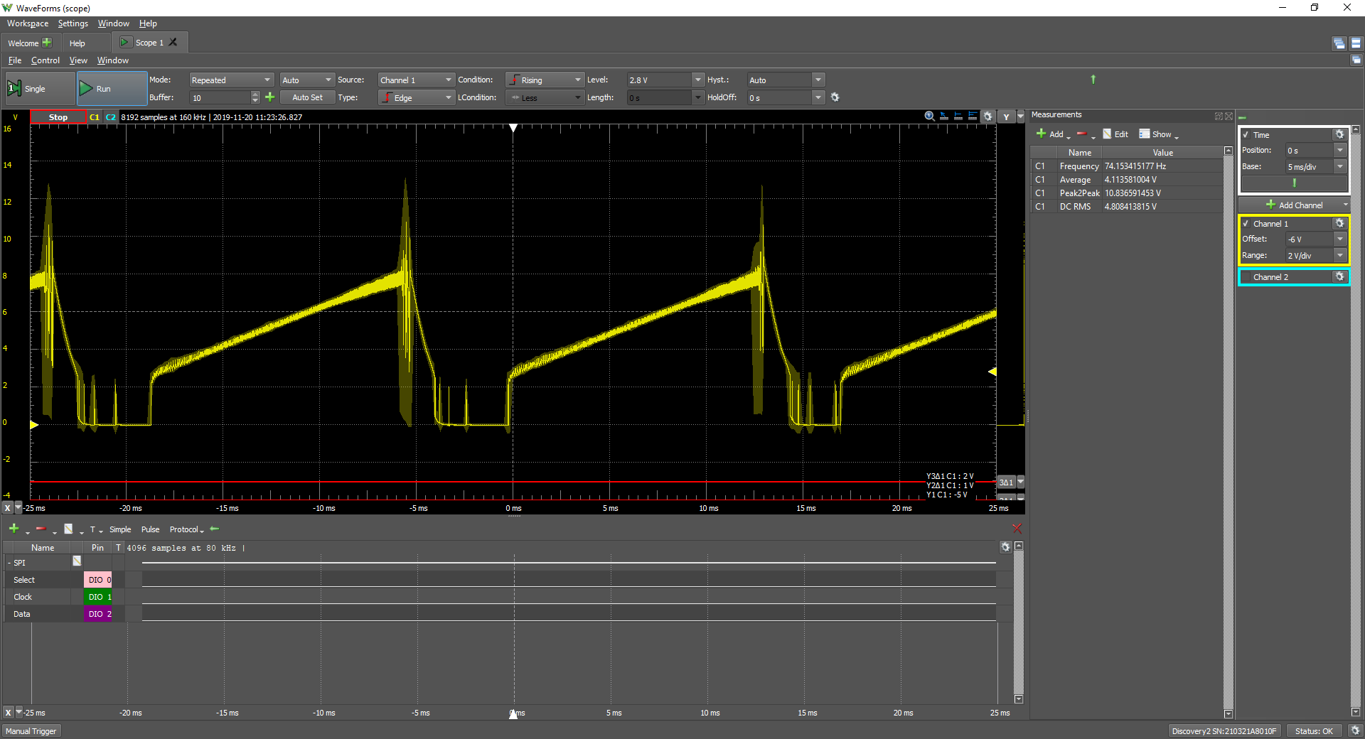
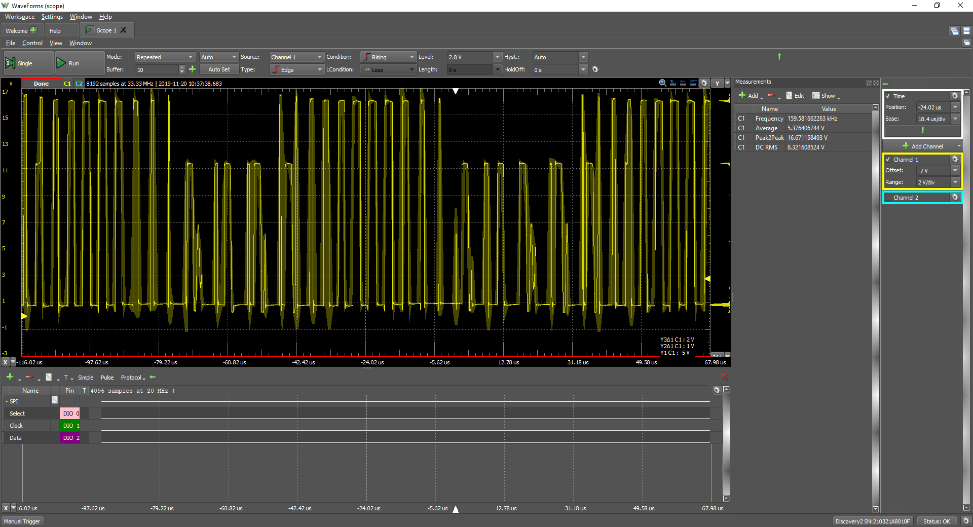
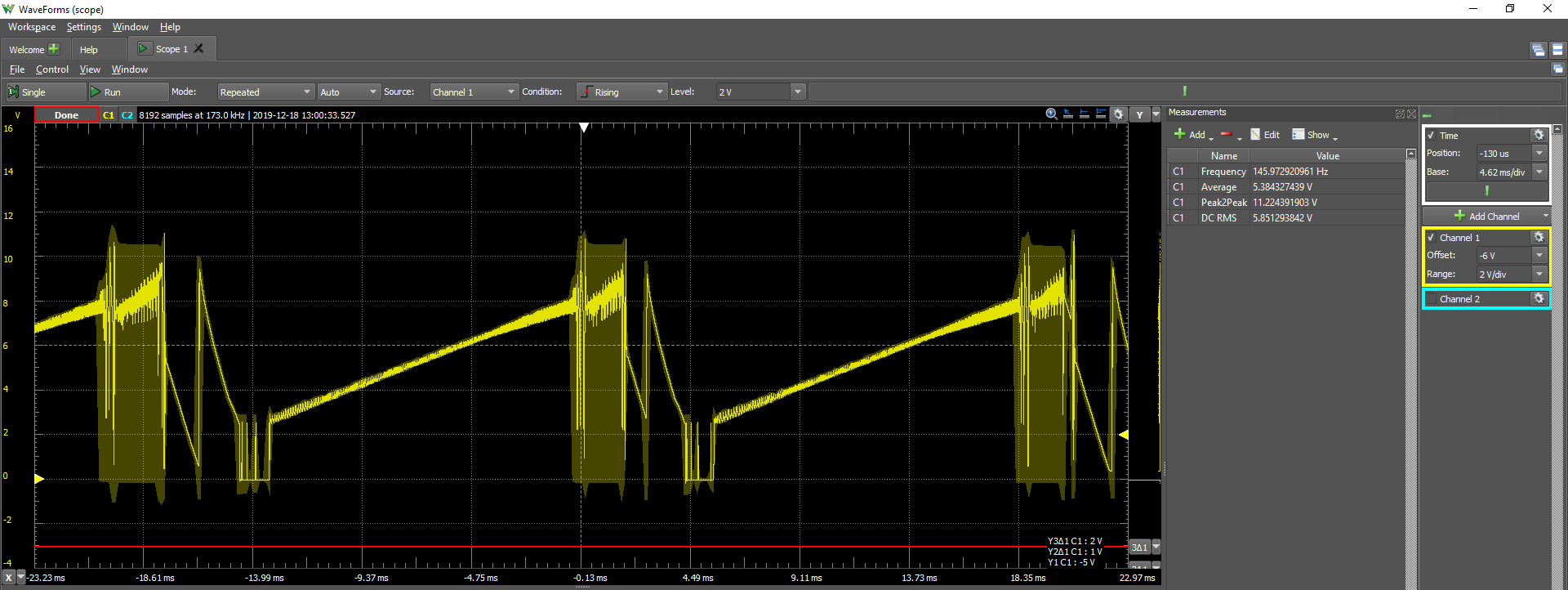
- HDRV1 is showing as a noisy ground signal. Even after disconnecting all components on its net, its still sits at 0. See scope below.

- I have 2 boards built up that have the same current draw/results/issues

- When i pull the enable pin to ground, my board draws 0mA, so it appears that current is not leaking outside of the IC

- I have reflowed majority of the components at least once and tested everywhere possible for shorts

I created the following table of observations:

Pin Num Devboard Custom board I/O Function
1 2.23 2.3V I Enable
2 11.7 10.7 I/P Vin
3 11.6 Noisy 11.8 I Vin Sense
4 1.69 1.78 I Mode
5 0 0 I Dither
6 1.21 0 I
7 0 0 I
8 1.16 1.16 I SoftStart
9 1.39 3.23 O Compensate
10 0 0 G Gnd
11 0.8 0 I FB
12 10 0 I Vout Sense
13 10 0 I
14 10 0 I
15 0 Noisy 0 I
16 0 0 I
17 7.4 0 O PGOOD
18 10 0 I
19 16 6.8 O
20 16 6.8 P
21 0 Noisy 0 O
22 0 0 G Gnd
23 7.4 7.3 I/O/P Vcc - Out
24 10 0 I/P Bias
25 Switching Switching O
26 Switching 6.8V DC P
27 Switching 0 (Noisy) O
28 Switching 0 (Noisy) I

HDRV1 output signal: scoped

Schematic PDF for better resolution: http://a.uguu.se/7pnQPFOL2gKW_LM5176Customboard.pdf

  • Hi Ryan,

    Thanks for reaching out with your question and for using the LM5176.

    Can you please re-check the voltage on the RT pin (pin 6)? Did you use the same layout as the EVM? Taking a look at the schematic I don't see anything that sticks out as being incorrect.

    Have you checked with a different IC?

    Thanks,

    Garrett

  • Hi Garrett,

    I rechecked, and looked at the resistance this time (not just for a short) for this pin to ground, it was sitting at 33Ω. I replaced the wrong 33.2Ω resistor with the correct 33k and the psu now has partial life. I can hear the PSU ticking - likely the inductor and is hitting current limit on my bench psu set at 12V, 250mA.

    Looking deeper into it I can see the IC is constantly trying to start and its hiccup or similar has it stuck in a reboot cycle. Interesting to note that poking around with my probe at x10 on some of the pins, after a while it starts to regulate correctly with an output of 48mA @10V. There was no consistency to where I probed to get the system to meet regulation.

    Pin Num Devboard Now I/O Function
    1 2.23 2 I Enable
    2 11.7 11.4 I/P Vin
    3 11.6 Noisy 11 I Vin Sense
    4 1.69 1.7 I Mode
    5 0 100mv I Dither
    6 1.21 1.23 I R-Sync
    7 0 161mv I
    8 1.16 0 I SoftStart
    9 1.39 0 O Compensate
    10 0 0 G Gnd
    11 0.8 382mv noisy I FB
    12 10 7.9p2p I Vout Sense
    13 10 8p2p I
    14 10 90m noisy I
    15 0 Noisy 750mv p2p I
    16 0 600mv p2p I
    17 7.4 spikes to good for <1ms O PGOOD
    18 10 10v p2p I
    19 16 11v p2p O
    20 16 11v and p2p P
    21 0 Noisy noise ground O
    22 0 noise ground G Gnd
    23 7.4 7.3V - noisy I/O/P Vcc - Out
    24 10 ramping to 8v I/P Bias
    25 Switching Switching O
    26 Switching Switching P
    27 Switching Switching O
    28 Switching Switching I

    This is the typical waveform I get for quite a few of the IOs, the ramp up and sharp drop off. This is pin 15, CSG.

    At least at this point I can now see switching of my driver circuits. Below is pin 25 (LDRV1) then pin 27 (HDRV1)

  • Hi Ryan,

    Pin 15 (CSG) should not be going to 8V, in normal operation it should be very close to ground. It looks like there might be something wrong with your board.

    Do you have multiple boards? Are you seeing similar issues on other boards?

    Thanks,

    Garrett

  • Hi Garrett,

    Working through a bit more first off most of the noise shown is actually a poor grounding issue. Using a better reference we had much clearer signals, classic rookie mistake...

    Regardless, the power supply was still outside of regulation. We found that when we removed the input 100uF capacitor, by chance. Since then when supplying 12V input and 10V output, it regulates well. Placing a load on the device and increasing the input voltage as higher has 19V still works fine, though once we hit 20V+ it starts to draw twice the amount of current and at 21V stops regulating. A few other notes, it doesn't appear to work below 12V with a load and below 10V without a load.

    Another interest note was that when we were probing signals, the feedback signal didn't like be probed on our board at all, setting the scope prove at x10 so 10meg parallel load with ~10pF brought the supply out of regulation. By comparison, the development board regulated fine regardless of probes presence.

    It seems we have made some progress, though there is obviously something happening in our feedback circuit that is way to sensitive.

    Pin Num Eval board Custom board I/O Function Comment
    1 2.23 2.3 I Enable Should be greater than 1.22V to switch on
    2 11.7 11.7 I/P Vin Should be between 4.2 and 55V
    3 11.6 Noisy 11.7 Noisy I Vin Sense
    4 1.69 1.8 I Mode
    5 0 0 I Dither
    6 1.21 1.2 I R-Sync
    7 0 0 I
    8 1.16 1.19 I SoftStart
    9 1.39 1.45 Noisy O Compensate
    10 0 0 G Gnd
    11 0.8 380 Noisy I FB
    12 10 10 Noisy I Vout Sense
    13 10 10 I
    14 10 10 I
    15 0 Noisy 0 Noisy I
    16 0 0 Noisy I
    17 7.4 7.37 O PGOOD
    18 10 10V Noisy I
    19 16 16 O
    20 16 16 P
    21 0 Noisy 0 Noisy O
    22 0 0 Noisy G Gnd
    23 7.4 7.4 Noisy I/O/P Vcc - Out
    24 10 10V Noisy I/P Bias
    25 Switching Switching O
    26 Switching Switching P
    27 Switching Switching O
    28 Switching Switching I

    Cheers,

    Ryan.

  • Hi Ryan,

    as Garrett is out of office, I just re-assign the post to another expert supporting this device. He would reply these week.

  • Hi Ryan,

    It seems you circuit has issues in the buck mode.  It is not clear when you mentioned the 100uF capacitor.  Do you have issue with the 100uF installed, or not installed? 

    Can you re-capture the SW1 and SW2 when you see the problem?  Please also indicate the operating condition and anything you modified to be different from the schematic that you posted earlier. 

    Thanks,
    Youhao Xi, Applications Engineering 

  • May I assume the issue is resolved and I can close this thread?  You are welcome to re-open this thread by adding a new post or creating a new thread.

    Thanks,

    Youhao

  • Hi Youhao,

    Thanks for getting back to me and sorry I was taken away for other projects. I have attached a new schematic, the new one shows extra parts that are added and which ones are and are not populated. On the feedback circuit we use the 0R's as a possible bypass for the digital pot we plan to use once the circuit is working.

    When laying out the pcb in altium, I based it originally on the the design files of the eval board and replaced the components one at a time to match the components that we would typically use in the office. I am happy to send the design files on if you could provide me an email address that could make it easier to look through as well. This is what the laid out PCB looks like atm. Please note C48 is replaced by a 0R to match the eval board settings I have been working with. Also note that the eval board uses a 0R in place of R28, so I have tried to match its values. C1 component link: https://www.digikey.com.au/products/en?keywords=493-1668-ND

    I feed power in through the Green and Red cables, and draw a load on the white ones. Specifically when I mentioned that the input bulk capacitor was causing me an issue, you can see in the schematic R28. I have disconnected the resistor and replaced it with a short circuit, a bar. When I take the bar off, the power supply powers up into regulation (when placed in boost mode as mentioned in previous post). Though when it is reconnected, the power supply fails to go into regulation and starts constantly switching on and off, shorting my bench-top supply. The benchtop supply in these examples is set to a limit of 12V @ 350mA. 

    The additional circuitry on the side is not placed at all and is used to measure and control the voltage and flow of power in a battery charger styled solution.

    Following on from your other query, below is the scope measurements of SW1 and SW2. First off the 2 images below is when it is regulating correctly, input bulk capacitor is open circuit through R28. I figured that while the input capacitor is charging, it holds the input supply down for a few uSeconds or so, then the PSU starts to try and regulate in boost mode and gets stuck in this mode. On the other hand, if the capacitor is removed, the transient response is much quicker, so the PSU won't start in boost mode, but buck instead.

    SW1 above regulating well with 12V input, 10V output.

    SW2 above regulating well. with an input of 12V and output of 10V.

    On the other hand, after it has been regulating well and I drop the input voltage to 11V, the PSU goes out of regulation.

    SW1 above, 10us timescale, out of regulation. 11V input, 10V target output

    SW1 above, 4.62ms tmescale, out of regulation. 11V input, 10V target output

    SW2 Above. 4.62ms timescale, out of regulation. 11V input, 10V target output

    I hope the above helps and once again, to make it easier I can email or upload the raw altium cad files to a private area if you'd like.

    Looking forward to your reply,

    Ryan.

  • Hi Ryan,

    It sounds like your input power supply cannot handle the inrush current draw by the input capacitors. 350mA limit sounds too small. If you read our EVM user guide, you can see the recommended power supply capacitor. 

    Can you change to a bigger power supply?  The reason that I am asking this is, I am afraid the root cause is the limitation on you input power supply which triggers overloading protection mode and cannot sustain the supply voltage.  Lets rule out this factor and see if your circuit can operate normally.  Otherwise, we may be chasing a ghost.

    Thanks,

    Youhao