A related question is a question created from another question. When the related question is created, it will be automatically linked to the original question.
If you have a related question, please click the "Ask a related question" button in the top right corner. The newly created question will be automatically linked to this question.
I am pleased hear from you. I think you have to take care 2 points.
1, since the min delay time of OUTA and OUTB is 150ns, you can't get absolutely 0.5 duty cycle. But, You can change the R_delayset to design different delay time.
2, if you found that delay time of OUTA and OUTB is 150ns already, please check the driver delay time and the driver push- source current whether is enough to drive your mosFET. You can use driver which have greater current. and you can try to change driver Resistor value to lower.
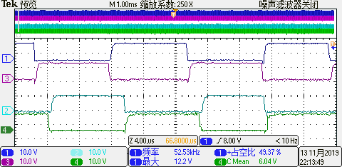
The first two pictures are normal situation. The Ton and Toff are alomost equal. The dead time is 300ns. (CH1-OUTA, CH2-OUTB)
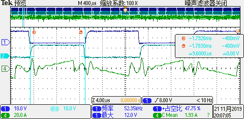
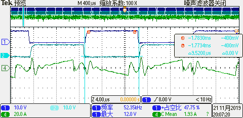
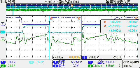
But the following two pictures are abnormal ones. The Ton of CH2 is 8.08us, the Toff of CH2 is 9.84us. The difference is too large. Also, the CH1's Ton>Toff. (CH1-OUTA, CH2-OUTB)
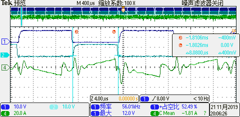
Not only the duty cycle of outA\B can be mistaken, but also outC\D can also be mistaken. As the following picture shows, CH1-outC, CH2-outA, CH3-EAout, CH4-the primary current of the transfrmer.
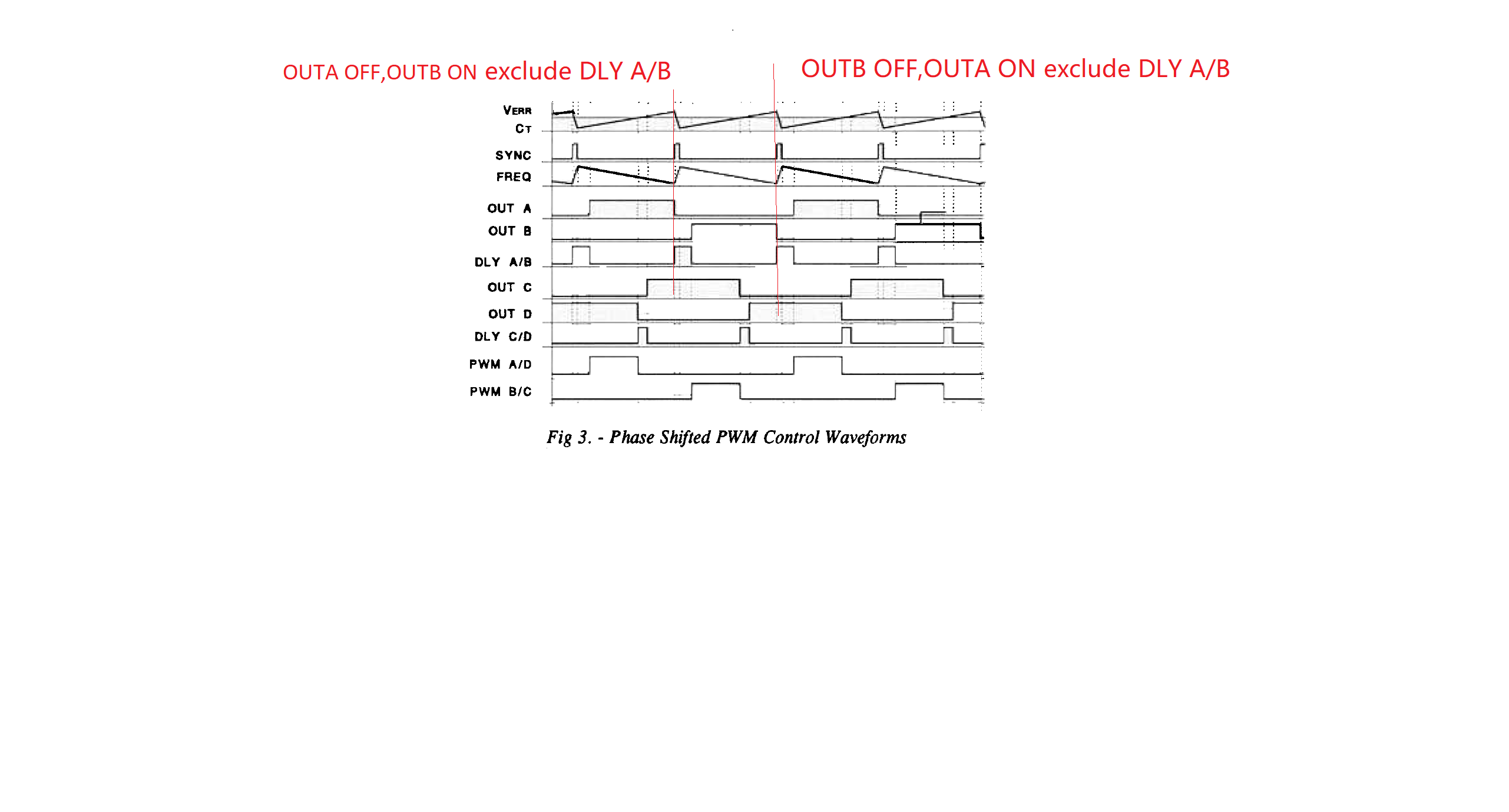
since there is no timing diagram in the UC3875 datasheet, I copy from other phase shift controller as attachment for you reference. according to the timing diagram, I you can get the information what is the decision conditions of the OUTA/B ON or OFF. the key is the SYNC and Freq waveform. so, can you please double check the waveform on the PIN SYNC(17) and Preqset(16) compare with the OUTA/B. you can show the waveform here if you are available.
If you find there is noise on these PIN, you have to find the noise source and fix it.
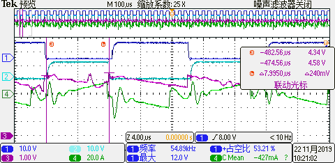
I have captured the pin(fset) as the following picture. CH1-OUTA, CH2-OUTB, CH3-fset. The waveform did have some noise that affected the timing diagram.
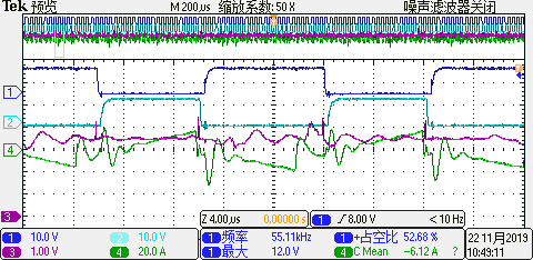
The following picture is the sync pin---CH3. It did have noise on this pin. But I don't know if it affect the timing diagram. In some place, the voltage of SYNC exceed the high voltage but the OUT is still high.
I don't know how to improve the chip anti-interference.
It is difficult that fix the noise issue through theoretical analysis. So, you have to try variety of way to solve this issue by yourself.
Here, I just give you some proposal according to my experience before. I hope it is useful to you.
1,You need to pay attention the function of ZVS is achieved. If there is hard switch situation, there is great current noise in the circuit loop. You can increase the delay time and increase the inductance of Lr to improve the performance of ZVS.
2, A good PCB layout is basic. So, double check you PCB layout and find the doubts you think. double check whether the signal GND trace and the power GND trace are separated.
I have tried VCC from outside aux DC supply, but it didn't seem to be useful. The phenomenon still esists. OUT A and OUT B almost remains to be 0.53/0.42 or 0.42/0.53.
Would you please reccommand some PCB layout of UC3875 application?
In only control supply, the waveforms are correct.
Also, in openloop conditions, the driver waveforms are correct. And I tried 200W load, it's still OK.
However, in closed loop condition, when I tried 100W load, the driver waveforms became abnormal. Sometimes, OUTA(~0.53) > OUTB(~0.41); sometimes, OUTB(~0.53) > OUTA(~0.41).
Many problems like this are due to noise injection caused by the PCB layout so it would be really good if you would share your PCB Gerber files with us so that I can review them. Please also include your schematic files. If you don't want to post them to this public forum then please send them to me at
I've been able to open the layout files - my apologies, I had forgotten that you had sent them to me. I've sent you some comments by email. The main thing is that the ground connections at the IC need to be improved.
According to Colin;s advice, I have tried to remove the IC, place a layer of Polyimide (Kapton) or other high temperature tape over the area occupied by the IC. Then place a copper tape over the Kapton and connect it to pins 12 (PGND) and 20 (GND), add a second layer of tape as an insulator. Then replace the IC.
However, the experiment result shows that the improvement does't seem to be useful to solve the problem of OUTA/B.
Now, I am wondering if there is a way that I only need to drill somewhere on the PCB to disconnect the power gnd with control gnd.
I will very appreciate it if you can offer me some advice.
I am not sure that the issue can be resolved if you just want to rework on you original PCB rather than Do the new PCB. Since you know that there are so much Parasitic parameters on your reworked PCB. It maybe make more noise on you PCB.
Could you please show the PCB picture after you reworked here?
This thread is opened long time. I have to close it now. we'd be pleased to discuss your issue with you in the further. If you have more question need to discuss, you can send email to me (Bliss-Zhou@ti.com ) and Colin. or you can open a new thread to discuss.