This thread has been locked.

If you have a related question, please click the "Ask a related question" button in the top right corner. The newly created question will be automatically linked to this question.

UCC28631: Bad Regulation / Burst Mode

Part Number: UCC28631

Dear Team,

our customer is using the UCC28631 in following system use case:

  • Vin: 350 to 450 V
  • Pout nom : 100W
  • Vout nom: 24V

I can share the customer's schematics and design file (Excel) via e-mail. Also with some more details about the transformer.

With a smaller load (Dummy of 5kOhm), they see following problem:

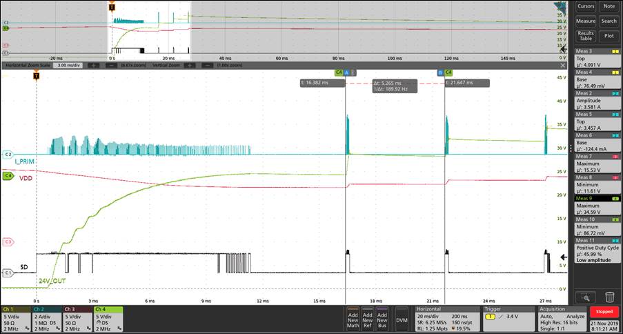
" The switching frequency and duty cycle suddenly become too large, as if they stop being regulated and there is no apparent reason why does it happen. The scope plots (CH1:SD, CH2:I_PRIM, CH3:VDD, CH4:VOUT) shown below depict the behaviour that I try to describe.

The supply start and output is regulated to 24V. Suddenly the switching stops, the voltage starts to drop, and when the regulation picks up, the switching frequency is already 120kHz and the duty cycle is ~60%.

This “burst” of pulses continues, with a separation of 5 ms, increasing the output voltage until the OVP kicks in. The zoomed in scope plot show that the error code is 20, and also shows how the duty cycle and switching frequency change."

Different test points:

  • Adding 680uF capacitance to the output also helps to decrease how often the “spurious behaviour” occurs, but it still does occur
  • 50Ohm @ 200V works most of the time. Increasing the input voltage will make the problem appear again.

Could you please help us understand what issue might cause the problem?

Thanks and best regards
Martin

CH1:SD, CH2:I_PRIM, CH3:VDD, CH4:VOUT

Conditions:

  • Rload = 5kOhm (applied externally)
  • Vin ~= 120V (the input voltage is actually ramping to 350V but the supply already kicks in at 120V)

  • Martin

    Could you send me the excel file and schematic to review?

    In the meantime Table 3 on page 42 of UCC28631 datasheet shows a list of all fault conditions that could cause UCC28631 to shutdown.  In the waveform you shared it looks like SD pin is getting pulled low.  For UCC28631 if SD pin is pulled low for 125us it will trigger a fault shutdown.  SD pin is typically used with an external NTC for over temperature protection or external shut down.  During normal steady state operation it should have a DC value rather than the PWM pulses that are shown on the waveform you provided.  I recommend that you review the circuit connected to SD pin to make sure it's operating as expected.

    Best Regards,

    Eric

  • Hi Eric,

    Thanks for your answer. Im the costumer, so I guess it is better that I answer directly to you  and I hope you received the schematics from Martin already. regarding your answer I have the following comments:

    • As it can be seen in the schematic, the SD pin was left floating. Assuming that open pin will not trigger any error by being open (table 4 page 43)
    • My understanding of the behaviour (of the SD pin) that can be seen in the scope plots is that at low power modes “the internal SD pin pull-up is disabled” (note (3) page 8), so I think the SD pin being pulled low is more a result of the disabling, rather than the cause. Also, the error code 26-(external overtemperature fault (SD pin pulled low)) would appear, and no error code appears afterwards, not until OVP is reached.
    • This is a remark on the datasheet: figure 37 show that the current source for the pullup is 210mA however it should be 210uA right?
    • I have made now two changes to the circuit
      1. I removed the R2CD snubber part and replaced with a zener clamp, now I am able to startup with 5kOhm load, but only at low input voltages it can maintain regulation. The assumption is that the output voltage was not reflected correctly to the bias winding due to current  still flowing through the primary after the FET was turned off. So this is an improvement but as soon as I start rising the input voltage (>160V), the “spurious behavior” of high duty cycle (~70%) and high switching frequency (120Khz) appears again. Now the OVP is not hit, but the output voltage have these spikes, that clearly indicate that the chip has stop regulating correctly
      2. I added a 470k resistor to the SD pin just to be sure, but it didn’t improve anything, I can see the SD pin still going down, always at the same time that the switching stops.

    After looking at the schematic do you have any other ideas why the chipp will suddenly stop regualting the output and go instantly to this high-switching frequency high duty cycle mode?

    k.r.,
    Omar

  • Omar

    Yes, I have received the schematics from Martin.  Since the email includes information that's needed to help resolve this issue that cannot be posted on E2E, we will continue to provide support by email.

    Best Regards,

    Eric

  • Hi Eric,
    Please let me know if I can send you more mesaurements, or information about my design to make it easier for you to help me out.
    Thanks!