This thread has been locked.

If you have a related question, please click the "Ask a related question" button in the top right corner. The newly created question will be automatically linked to this question.

TPS65917-Q1: TPS65917-Q1, DRA726 EVM and PMIC_REGEN_DDR issue

Part Number: TPS65917-Q1
Other Parts Discussed in Thread: DRA726

Hi All,

I am reviewing the TPS65917-Q1 setup in the DRA726 EVM and I am not understanding several things:

  1. I am assuming the PMIC is working with PRWON and NSLEEP instead of with POWERHOLD and POWERGOOD, right? This is not clear as the EVM PMIC is using OTP 3D instead of 30,31,32 or 33 versions.
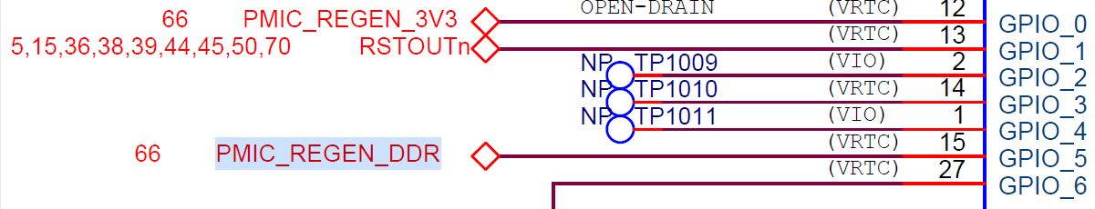
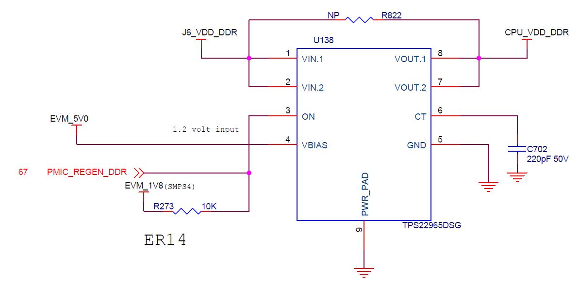
  2. Why is PMIC_REGEN_DDR (output) connected to POWERHOLD (GPIO_5, input)? Why is NOT connected to REGEN2 (GPIO_4, output), which is the output intended to be used for this tasks?

Thank you very much.

Regards,

  • Guillermo,

    Hi, there are 2 ways to turn on the PMIC:

    1. A push button on the PWRON pin, followed by either DEV_ON bit written high or POWERHOLD going high

    2. POWERHOLD goes high (like an enable signal)

    For this processor, the 0x30, 0x31, 0x32, or 0x33 OTP settings can work. To pick one, you need to know your expected currents and system requirements. You can use the NSLEEP OTP options if you want the ability to use GPIO_6 to put the PMIC in a low power mode, where only DDR is powered. You can use the POWERGOOD OTP options if you want the ability to use GPIO_6 to monitor the SMPS rails.

    REGEN2 is used to enable the DDR, however, it is open drain. This means that it needs a pull up resistor to be able to be driven high. I am guessing that the EVM is pulling up this GPIO_4 to POWERHOLD. We recommend not pulling it up to VCCA because the GPIO will go high before the OTP loads then go low again before the power sequence starts. If there is a 1.8V or 3.3V rail that turns on before GPIO_4 (like SMPS4), you can use that as the pull up.

    Please let me know if this answers all your questions.

    Thanks,

    Nastasha

  • Hi Natasha,

    Thank you very much for your explanation.

    However, and despite the fact I understand your assumption about whats going on in the EVM and it makes sense to me, It not seems to match what is actually going on in the schematic. What I see is:

    • GPIO_4 (REGEN_2) is only connected to a TP that it is, in fact, not populated.
    • GPIO_5 (POWERHOLD) is connected to PMIC_REGEN_DDR and pulled up to 1V8 (SMPS4)
    • The schematic I'm taking a look is 517502 REV D

    PMIC side:

    VDD_DDR driver side:

    Best regards,

  • After investigating Jacinto6Eco PDN & TPS65917 OTP history in question, it looks like the “Jacinto6Eco EVM PDN #1” diagram shown in “Power Solutions Rev 1.43” ppt was mis-labelled since it was really more of a hybrid PDN that showed portions of EVM PDN but with "End Product" optimizations. I can see how this would be confusing.

    Therefore, I've created a new "EVM PDN #0" diagram aligned to Jacinto6Eco EVM revD SCH and updated "PDN #1" to show an End Product PDN that closely resembles the EVM. Please review the new "Jacinto6Eco_SoC_Power_Solutions_Rev1.47" uploaded to CDDS and attached here for your quick reference.

    Let me know if you have any follow-up questions...:)

    BillJacinto6Eco_SoC_Power_Solutions_Rev1.47.pdf

  • Hi Bill,

    Thank you very much for your detailed explanation. All my doubts were solved!

    Regards,