Hello:
Recently, a 100W half-bridge power supply was made with reference to TI's LM5035 sample. The circuit schematics and manuals recommend the same circuit.

Produced 50 prototypes, a strange phenomenon appeared. There are 25 circuits that are normal, and 25 of them burn the MOS tube when they are powered on, and most of them burn the secondary rectification MOS tube, and also burn the primary MOS tube.
After replacing 25 burned MOS tubes with the prototype, the power supply is normal.
After the power supply is normal, I tested the drive waveform of the MOS tube and the voltage of the DS terminal when the prototype was started, which is normal.
Later, the product was subjected to high temperature experiments. During the experiment, 4 of the original 25 good MOS tubes were damaged, 2 was only damaged after one day of high temperature work, and 2 was just damaged by no-load power-on. The secondary rectification MOS tube has broken three, and the primary MOS has broken one.
I am very confused now. The tube is genuine, and the waveform is normal when the power supply is stable. After the MOS tube is broken, it will be replaced by a new one, but I can't find the reason. I don't know where it is. Now my heart is very low, maybe someday the prototype will fry the MOS tube.
Also ask the seniors to point out the maze, how can I find the reason? What other factors may cause this kind of good or bad?
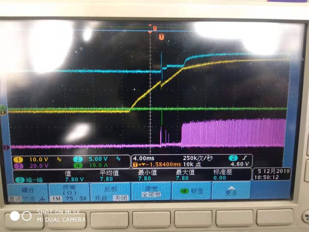
 Hello, the above figure is the waveform when starting without load. Yellow is the input voltage waveform, blue is the output voltage waveform, green is the output current waveform, and pink is the DS waveform on the secondary MOS tube.
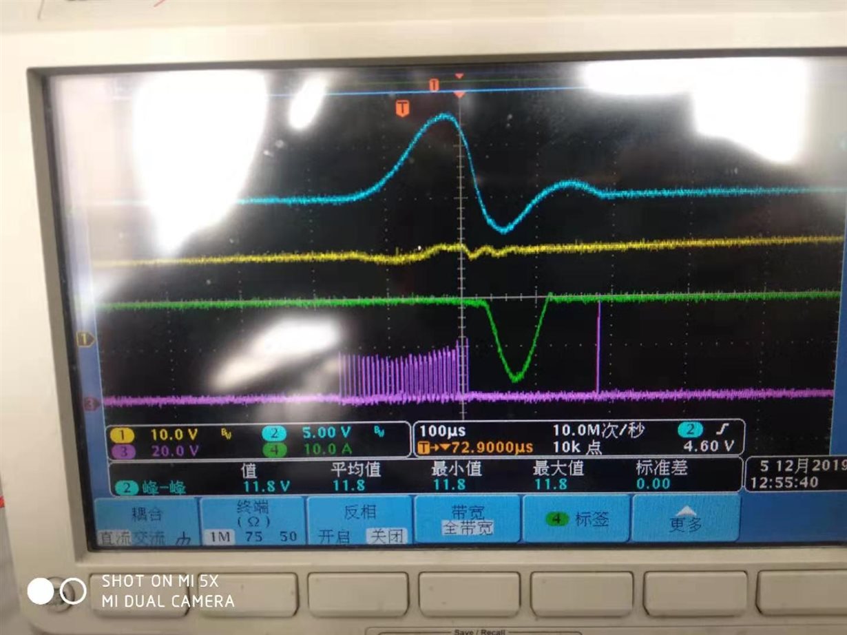
When starting, the input voltage will drop. At this time, the blue output voltage will have a spike, and the green output current will have a reverse current spike. The following figure is a detailed expanded view:
The output voltage spike will rush to 8V, the normal output voltage is 5V, the green reverse current spike is about 15A, and the width is 100us.
I know this waveform is abnormal, but I don't know if this reverse current spike will cause the secondary MOS tube to be damaged.
I use a vishay tube, 80V withstand voltage, 60A through current. But I can't find the data of the reverse current in the chip manual.
I later increased the soft-start time and this tip disappeared.
Is the 15A reverse current tip flow path the DS parasitic capacitor-output capacitor of the L2-T1 secondary winding-Q4Q5Q6Q7?
Will this 15A reverse current break the MOS tube? I tested this batch of products, and they all had this reverse spike when starting up, but some MOS would be broken and some would not.


