This thread has been locked.

If you have a related question, please click the "Ask a related question" button in the top right corner. The newly created question will be automatically linked to this question.

LP38798: High Voltage, Low Noise Linear Regulator

Part Number: LP38798
Other Parts Discussed in Thread: TIDA-01371, , LM317, LMS8117A, LM1117, TLV431

Hi,

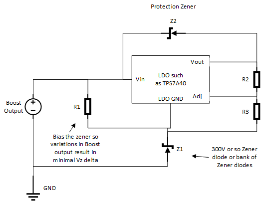
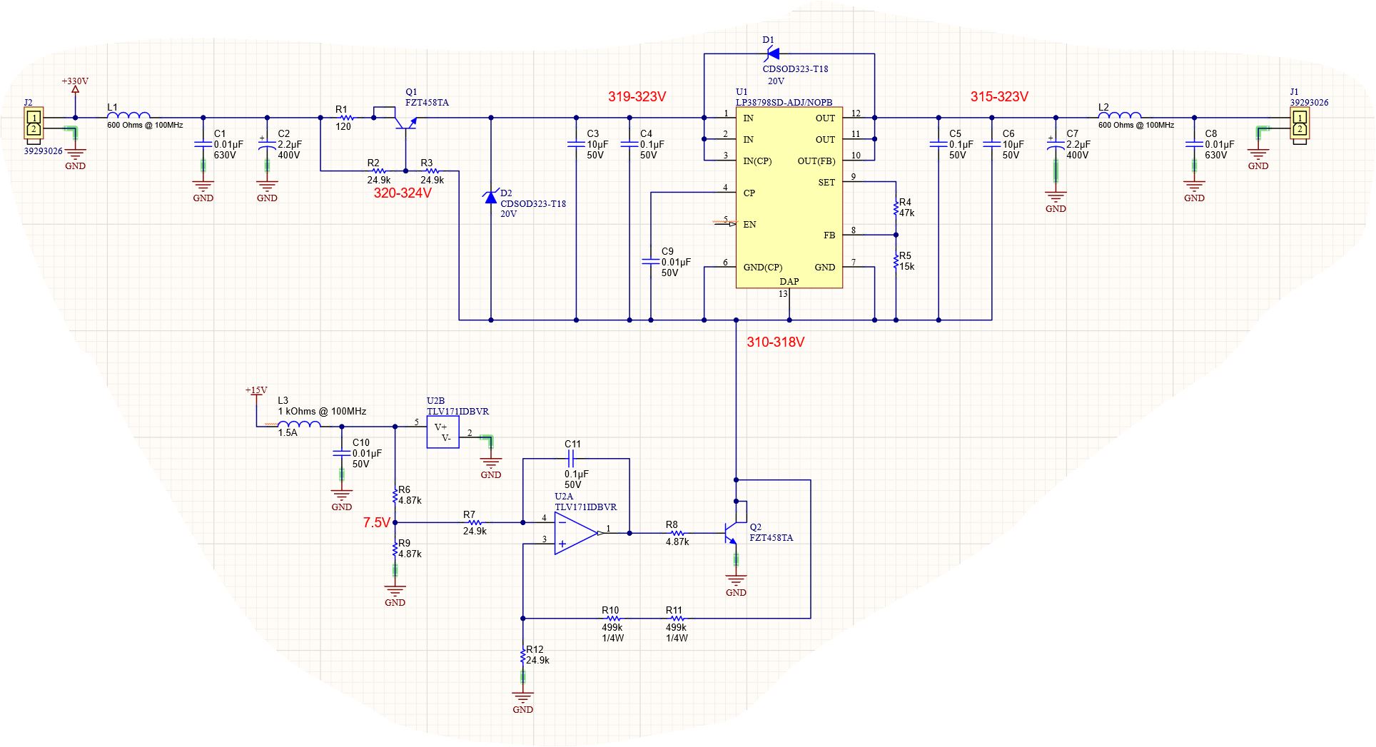
I am trying to design a low noise, high voltage linear regulator. It is being used to clean up a switching boost converter operating at 400kHz. I've experimented with the LP38798 in a floating ground circuit like the TIDA-01371 design. This works in that it provides a predictable and stable DC output voltage, but the low frequency AC noise is too high for my application (pro audio tube supply). I think this is due to the high low-frequency AC gain due to the integrator (U1). Of course any noise from the integrator stage gets passed right to the virtual ground node and through to the output of the regulator. 

I am wondering if I am missing anything with this floating application re: noise OR if there are alternate high voltage linear regulator configurations that might be more promising. I am interested in the floating arrangement of a 3-term adjustable regulator shown here: http://www.ti.com/lit/an/snoa648/snoa648.pdf - but I am wary of the high frequency ripple rejection of the LM317. 

Overall specs required below:

Vin = 330V (I have control over this parameter)

Vout = 320V, +5V/-10V 

Iout = 10mA nominal, 20mA max

Source is boost converter operating at 400kHz. 400k ripple and higher harmonics from switching as expected. Boost converter does not have low noise voltage reference, which is one main reason an active regulator is needed. 

Thanks! 

Ian

  • Hi Ian,

    We will need a few back and forth discussions to reach a conclusion on this LDO problem.
    It may be helpful to see the schematic of your design so far.
    I wouldn't need the boost converter, just the post regulation schematic.

    The floating reference topology LDO's include the LM317, LMS8117A and LM1117.
    At 400kHz the PSRR is poor in these older devices.
    One option is to reduce the switching frequency of the boost converter, then use the floating reference based LDO as shown in the App note you linked (http://www.ti.com/lit/an/snoa648/snoa648.pdf).  However I don't know what flexibility you have with the switching frequency.

    Some questions:
    1. What is the worst case ripple from the boost converter, and by how much do you wish to attenuate it?  Also, what is the min / max switching frequency?
    2. How are you generating the low voltage for the rail of U1 in the TIDA-01371?
    3. Can you increase the switching frequency of the boost converter, and add an LC filter prior to the Op-Amp to attenuate the noise?
    4. If noise is being amplified by the Op-Amp, would it be easier to use the following basic circuit for the LDO?  All of the other features would have to be added, such as capacitors and additional protection circuit elements. If the zener diode is not optimum, then perhaps a discrete LDO using a TLV431 and a BJT as the pass element. 

    Thanks,

    - Stephen

  • Hi Stephen,

    Thanks

    for the response. I've attached a schematic: 

    Answers to your questions:

    1. Worst case ripple from boost converter is 120mV @ fsw (400kHz). I have started on the low side of the switching freq range. Converter can operate up to 2MHz.

    What's interesting is that sub-fsw noise appears worse than fsw noise. I'm seeing audio-band noise of approx 250mVpp from the converter output. 

    I'd like to attenuate the audio-band noise by 50-60dB. I am working with the DC-DC converter vendor on my design to see if there's a way to mitigate audio-band noise at the source. I'd imagine the converter internal Vref might not be the quietest. 

    2. The DC-DC boost converter is fed from a 15VDC power module. I've used this same rail for U1. I've also tried a separate, lower noise rail for U1 with no change in HV Linear reg output noise. 

    3. The more I've thought about it, is it possible the integrator driving virtual ground node topology might just be incompatible with low, low-frequency noise? I think due to the inherent high U1 gain at low frequencies?     

    4. I am considering a discrete LDO. However I may also investigate using a LD1086 (not TI part, sorry) as a floating 3-term device. It's datasheet claims very good HF ripple rejection. 

    Any other ideas? 

    Thanks for your time, I appreciate it! 

    Ian 

  • Hi Ian,

    If the 15VDC power module is digitally controlled, then the limit cycling of the ADC in the feedback will cause low frequency, broadband noise.
    This will be in addition to the high frequency switching action.
    I have some experience with digitally controlled power supplies and the low frequency noise I saw was from 1KHz to 30KHz, with the spurs being quite substantial (on par with the switching frequency fundamental in some cases).
    You may want to review the power module architecture to make sure its noise is sufficient for your design.

    I agree with you on the inherent difficulties of a low noise high voltage output using this architecture.
    The LDO will certainly provide PSRR from its input to output. 
    The virtual GND may not have the same noise reduction, which the LDO is riding on.
    So I would expect the total noise to be lower, but perhaps not by a lot given the large differential from the virtual ground to actual GND, vs the LDO output to virtual GND.
    What you need is a method to lower the GND noise, as you have already discovered.

    We can discuss methods to reduce noise surrounding the U1 circuitry (use LDO's such as TPS7A4701 powered off 15VDC to provide U1 rail and 7.5V, proper placement and layout to reduce noise, short loop areas in the layout, an effective electric field shield by making layer 2 GND underneath U1 circuitry or layer 2 is the LDO GND underneath the LDO circuitry).

    But the boost converter noise can still make its way into the virtual ground with this architecture.
    If you can reduce the ripple voltage as much as possible from the boost converter, then you may be able to use a zener as I previously showed with improved noise results than this existing architecture.  With a tight tolerance bias resistor (1% or better), the Iz will not fluctuate significantly, which depending on the zener may give very little change in zener voltage.  Zener tolerances are sloppy but the idea is that would be a very low frequency change based on temperature, and less than ripple from the switching converter.

    Another option is to design a discrete LDO using the TI TLV431.
    You would be able to compensate it yourself to achieve the desired ripple rejection, although this is more labor intensive than an IC, and may not meet your schedule.

    I looked at the LD1086 and the TI LM317.
    Be aware that the LD1086 requires ohms of ESR for stability, so transient response will suffer if that is important to you.
    Ceramics will not work and even tantalum capacitors may be insufficient.  You will probably need aluminum electrolytics.
    The LM317 does not have this limitation. The PSRR of both devices look to meet your 50-60dB of attenuation in the audio frequency range.

    Perhaps you could also try placing two LM317 LDO's in series to double your PSRR, assuming your design constraints will give you enough headroom.

    Please consider these options and let me know if I can provide additional support.

    Thanks,

    - Stephen