This thread has been locked.

If you have a related question, please click the "Ask a related question" button in the top right corner. The newly created question will be automatically linked to this question.

LM3409EVAL: Limiting instantaneous current when using the LM3409 Eval board

Part Number: LM3409EVAL
Other Parts Discussed in Thread: LM3409

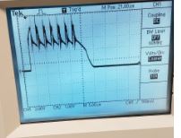
We are using the Eval board in PWM mode to drive a laser diode.  I have placed a scope across the output of the eval board to get the shot seen below.  The laser diode does lase and it changes brightness with changes in duty cycle.  Where my question lies is why are there spikes on the waveform? I would like a clean square wave. And second what is the instantaneous current peak.  The laser manufacturer has told us that any currents above 700mA will damage the semiconductor material as well as the coating on the faces.  The LM3409 is controlling the laser current to an average of 1A max, but it is not just the average current that is an issue but also the instantaneous.  We want to know if there is a way to limit the peak current.

In an attempt to better understand what is happening we inserted a 1 ohm resistor in series with the laser and measured the voltage on either side. The noise was terrible, but using the scope math function we subtracted the two signals and got a smooth triangle wave with a peak of 1V. That would indicate a peak current of 1A.  We also placed a snubber across the output of the driver board with various caps and 10 ohm resistors.  The output changed but the spikes remained. This tells me the spikes are not noise but are part of how the driver is operating the laser.  Any information about what is going on and how to limit the max current (instantaneous) (There is a way to change the average from 1A to 700mA in the datasheet), would be helpful.

  • Hello,

    The EVM is setup to run 1A average, there are equations in the EVM document showing 1.22A peak and 1.02A average by the calculations.  This can be changed a few ways.  Viadj can be used to lower the average current.  Rcs can also be increased to lower the current.  A capacitor can be added in C5 position to reduce the current ripple, the inductor value can be increased or the off-time reduced.  These are all part of the design equations.

    As for the current spikes, how are you connecting the oscilloscope to the output?  Since this is a switching solution noise can be picked up in the scope probe loop.  This can be checked by connecting the scope probe to where the ground is connected to see if there are still noise spikes.

    C5 can be added to reduce current ripple and current spikes if they are real.  A 0.1 uF may make a difference, if more capacitance is needed a 1 uF or larger can be added.  The current ripple reduction related to C5 has to do with the series impedance of the load.

    Changing R4 to 0.27 ohms will reduce the average to 0.7A however the peak will still be above, C5 may reduce this enough if large enough.  Changing R4 to 0.35 ohms will reduce the peak to 0.7A however the average will be lower than 0.7A.

    What capacitor value was used with the snubber?  If the current spikes are real the 10 ohms in series may not do anything.

    Best Regards,

  • I ADJ: We first used R5 pot to adjust the current, but it was too sensitive with a 1 turn POT. So we switched to a PWM at J1.  The PWM high goest to the enable pin and gnd.  That is how we were running when I took the scope shot posted.

    Snubber: I tried 500pf in series wtih 10 ohms across LED+ to LED-.  Also tried 0.1uF and 10 ohm.  They both reduced noise and ringing at transition points, but neither changed the spikes seen above 4.5V.  They are always there. At low duty cycle there are fewer of them. At higher DC the number increases but the distance between them is about the same.

    Scope: The Scope probe gnd is connected to LED- and the tip is connected to LED+.  This is a standard 10x probe with the gnd connected about 2 1/2 inches behind the tip and is about 3 inches long, so there is a loop when hooked up.

    I will order resistors and caps as you suggested and see what difference they make.  

  • Hello,

    Try connecting the tip to the point where the ground is connected and see it the noise is still there, I suspect it will be.  This way you are measuring the scope ground and if there is noise it's being picked up in the scope loop which is common.  Making a short ground path to the probe ground will reduce this.  They make scope probe tip sockets or you can create something of your own with solid wire (and removing the scope tip cover to expose the metal to wrap the wire around.  You can also try measuring out where the LED is away from the inductor and switch node.

    Best Regards,

  • Here is the signal measured across the diode:

    Then I took the probe tip and connected it to the same point on gnd where I had the probe gnd:

    As you can see the noise on gnd is about 20x smaller than the noise seen on the signal. Which is to be expected from a square wave switching at 5uS intervals. I do not believe these spikes are noise but are actually part of the control system in the chip.

  • Hello,

    This is a buck converter that is peak current regulated with an off-time that adjusts to keep the ripple amplitude constant with a varying output voltage.  The inductor current will look like a sawtooth or triangle wave in continuous conduction mode provided the output voltage doesn't vary significantly.  If the load is a fixed voltage with a dynamic impedance such as an LED it will look like a sawtooth or triangle wave also.  Try changing your load to LEDs or several series diodes to see if the current looks correct.  Also, the recent waveforms do not look like the oscilloscope picture at the top.  Also try installing C5 as mentioned above.

    Do you have an oscilloscope picture of the top waveform that is not AC coupled?

    What is the switching frequency?

    Best Regards,

  • Hello,

    I haven’t heard back from you, I’m assuming you were able to resolve your issue.
    If not, just post a reply below (or create a new thread if the thread has locked due to time-out)

    Best Regards,

  • Hi, so there are a few things. First I don't have access to the equipment right now, so I can't get the scope shot your requested. But I also don't see the need for none AC coupling. The reason I switched to AC coupling was because with DC coupling, the noise was so small you could hardly see it. I coupled AC and increasing the resolution 20x so we could see it.  While a good idea, the noise we see is not from the loop in the scope probe, but from the fast square wave transition with a 5uS pulse width.  Those noise spikes (not the large pulses I asked about in the original post) being small and appearing only at the transition of the large current spikes.

    Second, the noise spikes, it has been suggested to me by another engineer, are at the switching frequency of the device.  He suggested that the device turns on, you get a rise in voltage until it conducts and drains the caps. Then it turns off and recharges the caps, which corresponds to a drop in the voltage signal.  Then it turn on and the cycle begins again. That was the kind of information that I wanted and could not find in the data sheet.  I had hoped to find it here but did not.

    Lastly, while this device may be great for certain applications, we were trying to use it for a laser diode driver.  We have decided that since we cannot limit the peak current accurately and have no way of getting photo diode feedback from the device to the switching power supply, that this device is a poor choice for our specific application and have decided to design our own driver.  

    Thank you for your help.  Hopefully we will be able to use a TI part in a future product.

    Sean